Keep chip designs on the level with CMP simulation and dummy fill optimization
This case study shows how rising CMP simulation quality can be leveraged to detect the position and type of planarity hotspots before manufacture and verify the planarity of a layout.
Anyone who has ever laid a floor, built a rock wall, or even hung a picture knows the importance of keeping things level. Whether it’s protecting house guests from vertigo, or ensuring the garden wall will stand for years, starting with and maintaining a level surface throughout are critical. Manufacturing an IC is no different.
Chemical-mechanical polishing (CMP) has long been used here to achieve the required surface planarity of wafers. Based on process requirements, foundry engineers define threshold criteria and rules for planarity hotspot detection in post-CMP surface profile analysis. Post-CMP topography variation often causes degradation of the circuit performance, while the depth-of-focus (DOF) requirement is critical for lithography of subsequent layers. As such, compliance with planarity requirements is vital to maintaining IC manufacturing technology scaling trends, and supporting device innovation. Particularly because of shrinking feature sizes, it is a first-order element in the dual damascene process used at advanced technology nodes for post-deposition surface planarization and subsequent layers-processing.
Design for manufacturing (DFM) flows use these criteria and rules set by the foundry to perform CMP modeling and simulation, hotspot detection, and analysis in the design flow for production designs. These CMP simulations predict post-CMP surface topography and thickness values. This allows DFM and foundry engineers to locate potential planarity hotspots on production design layouts and fix them prior to manufacturing [1].
One of the most common techniques used to fix planarity hotspots is the insertion of dummy fill. These comprise inactive metal that fills otherwise empty areas in the layout to provide a more uniform surface when applying CMP. However, given the almost infinite number of fill patterns that can be used, deciding which fill pattern will deliver optimal planarity results, particularly at 28nm and below, is challenging at best. Typically, multiple dummy fill patterns will be printed and processed on production and test wafers. Then the results will be compared to identify the best choice. This is a very expensive process, considering the time and resources required.
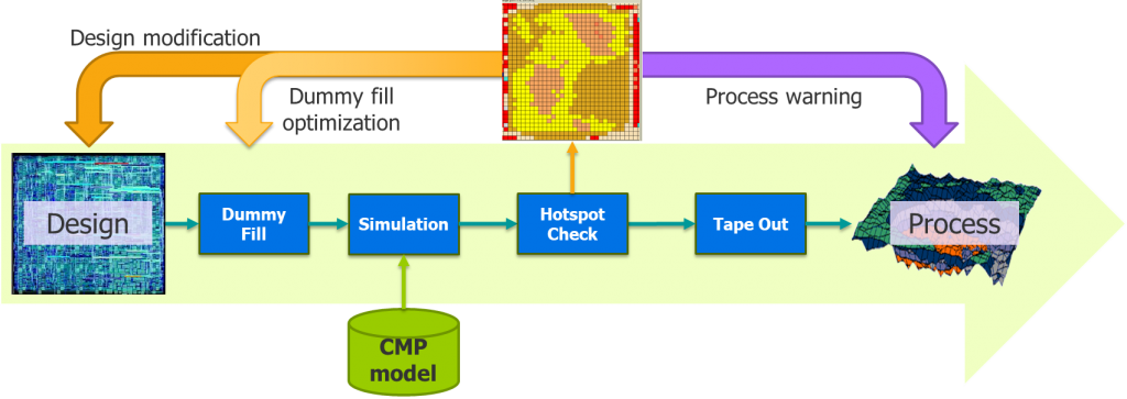
Development of faster, more effective, more efficient dummy fill optimization has long been a critical goal for production flows at foundries. Improvements not only help toward compliance with surface planarity requirements, but also enhance fixing of hotspots (e.g., bridging due to dishing, or metal thickness variation that affects timing and creates RC violations). Previous research has shown that a CMP dummy fill co-optimization method can help engineers select the best dummy fill deck for a specific chip [2]. At the SPIE Advanced Lithography 2020 conference, Huali Microelectronics, the Shanghai-based foundry, and Mentor, a Siemens business, presented a case study incorporating CMP simulation for both post-CMP hotspot detection and optimum dummy fill pattern selection [3]. Figure 1 illustrates the CMP simulation-based fill optimization flow.
In this context, the Calibre YieldEnhancer SmartFill DFM fill tool automatically inserts dummy fill to achieve planarity goals, while minimizing the number of fill shapes needed to reduce both the resistance variability and the additional capacitance created by the fill. CMP analysis tools like the Calibre CMPAnalyzer tool are then used to evaluate the results of CMP simulation and identify potential hotspots. Combining the two operations provides DFM engineers with the ability to fix planarity hotspots by optimizing local dummy fill insertion (although we note that the creation of automatic guidelines for hotspot fixing using original dummy fill target or shapes modification is still challenging).
CMP model-based dummy fill optimization
This method has two primary objectives:
- Predicting the post-CMP profile planarity and hotspots for multiple dummy fill rule decks through CMP simulation.
- Determining which deck results in the lowest number of hotspots
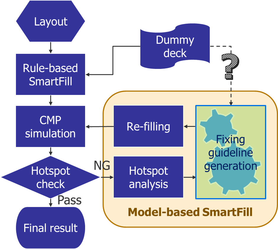
Figure 2 shows a schematic view of the proposed method.
The general flow consists of the following steps. While Calibre tools are referenced here, any tool that performs identical processes could be used.
- For a given layout, insert a dummy pattern using a rule-based dummy fill deck (e.g., rule-based Calibre YieldEnhancer SmartFill insertion).
- Run CMP simulation and detect hotspots based on the rules and threshold criteria defined for the manufacturing process.
- If hotspots are detected, locate and analyze hotspots (e.g., run the Calibre CMPAnalyzer hotspots clustering algorithm to detect and group hotspots to ease the hotspot fixing process [4]). If no hotspots are found, save any changes and move to the next step in the design flow.
- Run a hotspots fixing flow (e.g., model-based SmartFill modification) that fixes the hotspots using dummy pattern modification based on the CMP simulation results.
- For the selected area or cluster, use an engineering change order (ECO) flow with the Calibre YieldEnhancer SmartFill tool to control the removal of the original dummy fill.
- Refill just these areas with new dummy fill shapes selected based on analysis of the hotspot type (such as large dishing or erosion, low or high topography, surrounding pattern density, density gradient, design rule constraints, etc.)
- Repeat CMP simulation and check for hotspots.
- Continue the iterations until all hotspots are fixed, or it is no longer possible to optimize the dummy pattern.
CMP simulation and hotspot analysis
The CMP process creates three primary surface topology issues:
- Surface height variation
- Topology gradient
- Dishing for wide patterns
Based on the depth-of-focus requirements for lithography and other technology-related process requirements, planarity thresholds must be defined for the detection of surface weak points or hotspots.
Surface height hotspots are characterized by their coordinates on the layout and both local and long range geometric data. Variation in post-CMP wafer surface topography is highly dependent on the layout pattern, including the structures on scribe lines.
Because surface height variation is the major post-CMP condition that impacts lithography and can cause chip malfunctions, the focus of our case study was to improve surface planarity by optimizing dummy fill pattern selection using CMP simulations. To improve wafer surface planarity, optimal dummy fill pattern shapes and density should provide an almost uniform final pattern density distribution, with only small density gradients over the chip. Although both the original layout and dummy fill patterns impact planarity, engineers want to find the sweet spot that minimizes the changes in fill while ensuring that the changes achieve the targeted planarity.
To perform a CMP simulation, the chip area is usually divided into tiles of varying window sizes. For each window, geometric characteristics like width, space, pattern density, perimeter, and length are obtained from the chip layout [1]. Once the simulation is complete, these measurements can be used in conjunction with the simulated height data to identify potential hotspots.
Dummy fill target generation and selection
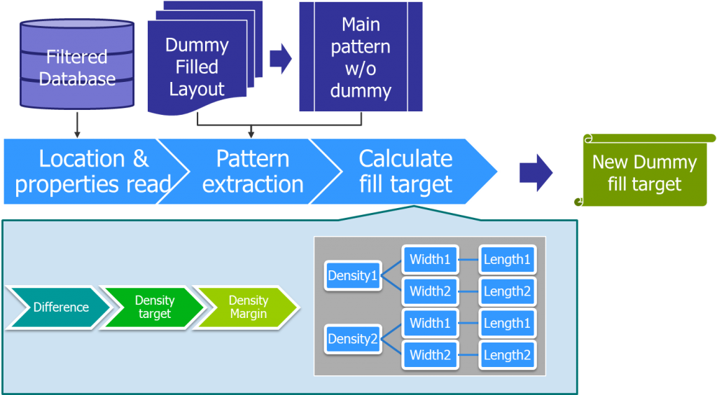
Based on the CMP simulation results, the next step is to generate possible dummy fill solutions and select the best solution. The dummy fill target generation flow is shown in Figure 3 and performs the following steps:
- Collect and analyze simulated height data and related geometry properties at hotspot sites, based on CMP simulations using the original layout with inserted dummy fill.
- Calculate the average of the surface height topography, then calculate height differences of hotspots from the average surface height. Use these differences as weights for further adjustments.
- Taking into account the topography differences, the pattern density filling margin of the original layout, and the correlation between the surface topography and the layout pattern, define the density target for a dummy fill deck.
- Generate a set of dummy fill decks with different patterns and the given pattern density target for different design of experiments (DOEs) for CMP simulations.
- For each dummy fill deck generated, use engineering change order (ECO) fill functionality to re-fill the layout or hotspot area (cluster) with that dummy fill deck, and perform a CMP simulation.
- From the resulting set of CMP simulation surface profiles, select the dummy fill deck that provides the best planarity with minimal or no hotspots.
Optimizing layout planarity for multi-layer layouts
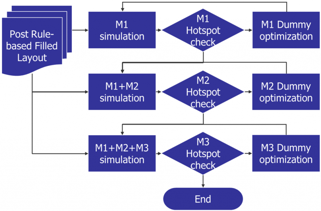
For multi-layer layouts, dummy fill optimization and hotspot resolution is completed layer by layer. Starting at layer M1 and continuing upward, the flow performs the following steps:
- Resolve planarity hotspots on the M1 layer using dummy fill optimization.
- Use rule-based dummy fill deck to fill the original layout.
- Perform CMP simulation on the filled layout and detect hotspots.
- Define areas (clusters) for hotspot fixing.
- Re-fill these clusters with one of the dummy fill patterns previously generated.
- Run CMP simulation and determine if the hotspots are resolved.
- Repeat steps d-e for all hotspot solutions.
- Select the filled layout that provides the best planarity as the final M1 layout.
- Use this M1 layer new topography for M2 layer dummy fill optimization.
- Resolve planarity hotspots on the M2 layer using dummy fill optimization by repeating the same steps, taking into account the underlying M1 layer topology for CMP simulations.
- Continue this procedure for all layers from bottom to top (Figure 4).
Results
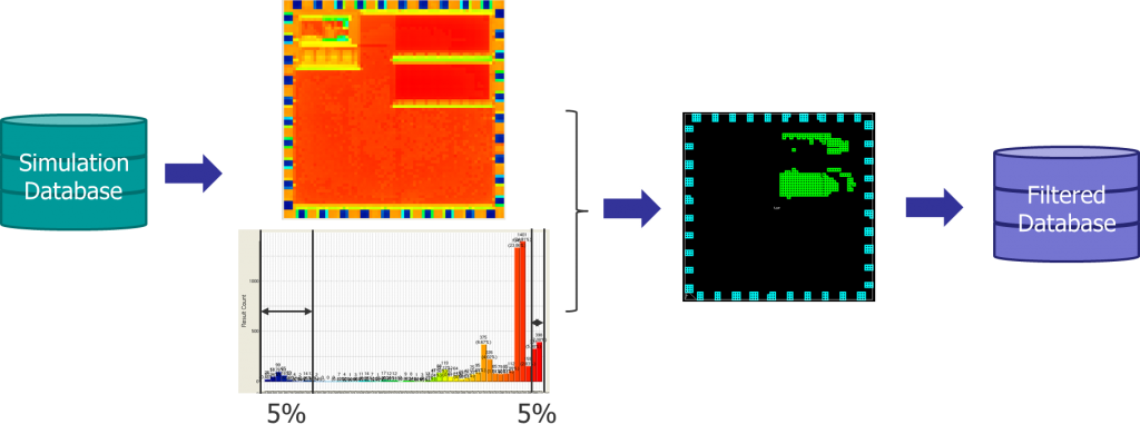
In our use case, ~5% of the total number of sites on a chip are hotspots. For our CMP simulations, we chose a 20×20µm window. For each window, we extracted the geometric characteristics (width, space, pattern density, perimeter, and length) from the chip layout [1], ran a CMP simulation, and filtered that information to identify hotspots (Figure 5).
We applied our dummy fill optimization method to fix planarity hotspots for back-end-of-line (BEOL) layers, creating a combined flow for a design with five layers (M1-M5). We then ran this method on the M1 layer to check the accuracy for a single layer case. The results are presented in Figure 6, showing the simulated surface topography colormap and simulated surface topography heights histogram before (without) and after dummy fill optimization.
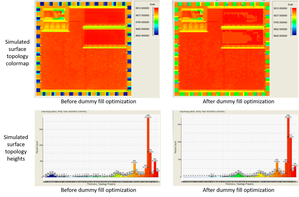
Figure 6. Surface planarity improvement by dummy fill optimization for M1 layer of a design with 5 layers (Huali)
We then tested the method on the M2-M5 layers, taking into account the topography accumulation of the underlying layers. The results for the M5 layer are shown in Figure 7. From the data in Figures 6 and 7, it is evident that using this dummy fill optimization method for each layer results in a significant reduction in surface topography variation and improvement in surface planarity.
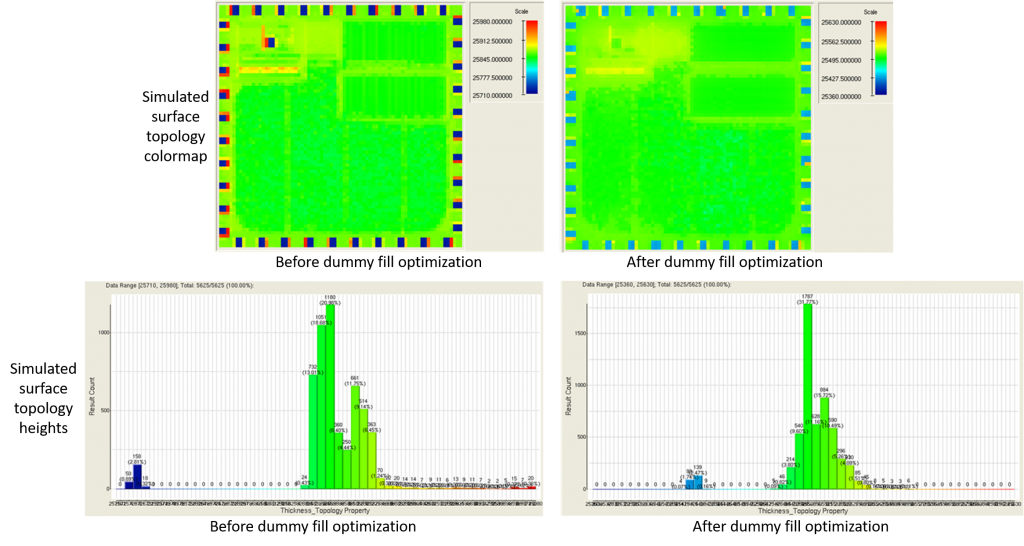
Figure 7. Surface planarity improvement by dummy fill optimization for M5 layer of a design with 5 layers (Huali)
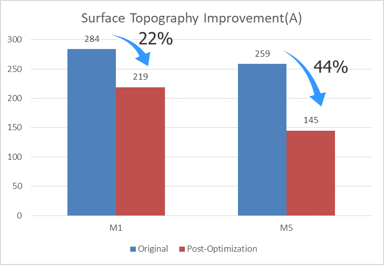
The ranges of surface topography variation before and after dummy fill optimization are shown in Figure 8. Topography variation was reduced by 22% for the M1 layer, and by 44% for the M5 layer. One reason for the significant improvement in the topography of the M5 layer compared to the original layout is the improvement of topographies of the underlying layers that impacted the final topography of the M5 layer.
Additionally, the histograms in Figures 6 and 7 demonstrate that both high and low surface areas were improved.
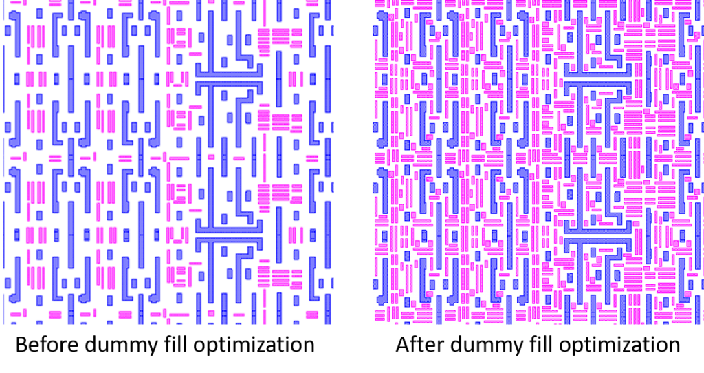
High surface height area: In this area, the original dummy pattern complied with DRC constraints, but the CMP simulation showed high topography hotspots, due either to the long-range effects of CMP or a multiple layers stacking issue. After dummy fill optimization, adding extra dummy patterns increased the pattern density and reduced density variation, leading to a reduction in surface height and the elimination of hotspots (Figure 9).
Low surface height area: The CMP simulation predicted over-polishing would create hotspots for a large Cu pad region. While it might be not possible to modify the main pattern to exclude this Cu pad area, this hotspot type can be fixed by slotting (i.e., adding oxide patterns inside the Cu pad to reduce Cu pattern density). Using the same dummy fill optimization method for slotting, an optimal oxide slotting pattern was selected and low topography hotspots were fixed (Figure 10).
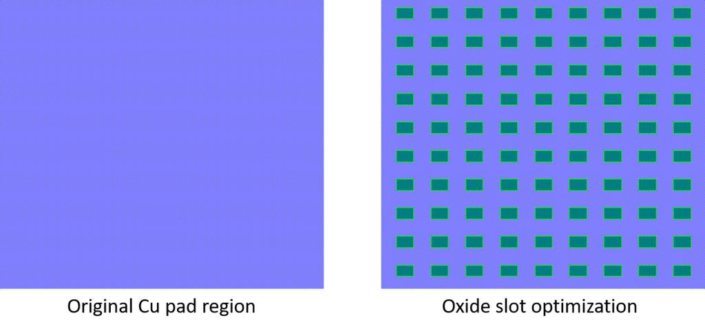
Figure 10. Optimal oxide slotting pattern generated for high-density Cu pad area to improve planarity (Mentor)
Conclusion
Surface planarity is a critical success factor in IC manufacturing. Adding dummy fill throughout a layout to reduce planarity variation is a long-established process, using pattern density and density gradient checking as criteria for dummy fill pattern selection. However, selecting an optimum fill pattern is currently a cumbersome and expensive process. In addition, because most design rules are set up to control single layer patterns, the criteria make it hard to accurately predict the effect of a selected dummy fill solution on the final surface planarity, due to CMP long-range effects and multi-layer stacking topography variation accumulation.
Modeling the CMP process provides engineers the ability to simulate a post-CMP profile and use this data to select the dummy fill pattern that provides the optimal planarity for a given layout. The quality of CMP simulation has increased significantly, enabling highly accurate detection of the position and type of planarity hotspots. CMP simulations are an important part of a DFM flow that predicts post-CMP hotspots prior to manufacturing, and provide a credible method for verifying the planarity of a specific layout.
A CMP simulation-driven dummy fill optimization method for achieving strong planarity requirements in advanced technology nodes was developed and tested using Calibre CMPAnalyzer, Calibre CMP ModelBuilder and Calibre YieldEnhancer SmartFill tools. The method uses CMP simulations to set dummy fill targets and select the dummy fill pattern that provides the optimal planarity for a given layout. To fix identified hotspots, an ECO fill method is used to remove the original dummy patterns around the hotspots and re-fill the area locally with the optimal fill pattern that satisfies the targets and achieves the required planarity. Application of the method to multi-layer designs showed good planarity improvement for all layers.
Just like building that rock wall, level is good in IC manufacturing. Implementing this type of dummy fill optimization method as part of the DFM flow for both single and multiple layer designs can reduce the time and resources required to find and fix planarity hotspots, while ensuring the most efficient and effective fill solution is applied.
For more information, download the whitepaper, CMP Simulation-Based Dummy Fill Optimization.
References
[1] Ghulghazaryan, J. Wilson, N. Takeshita, “Building CMP Models for CMP Simulation and Hotspot Detection,” mentor.com, July 2017, http://go.mentor.com/4TTwl.
[2] Yang Li, Rick Li, Peng Jiang, et al. “FEOL CMP modeling challenges and solution in 3D NAND”, Proc. SPIE 10962, Design-Process-Technology Co-optimization for Manufacturability XIII, 1096211 (20 March 2019); doi: 10.1117/12.2515167.
[3] Liwei Jiang, et al., “CMP simulation-based dummy fill optimization,” Proc. SPIE 11328, Design-Process-Technology Co-optimization for Manufacturability XIV, 1132817 (23 March 2020); https://doi.org/10.1117/12.2551681
[4] Ghulghazaryan, D. Piliposyan, V. Mkhoyan, M. Shoyan, S. Favre, J. Wilson, “Clustering of hotspots for dummy fill optimization using CMP simulations”, International Conference on Planarization/CMP Technology (ICPT) 2019, Hsinchu, Taiwan, pp. 139-140.
About the authors
Ruben Ghulghazaryan is a Research Engineer Principal in the Design to Silicon division at Mentor, a Siemens Business. He received a MSc in Theoretical Physics and Biophysics from Yerevan State University, and a PhD in Physics from Yerevan Physics Institute. He can be reached at rubenUNDERSCOREghulghazaryanATmentorDOTcom.
Jeff Wilson is a product management director for DFM applications in the Calibre organization at Mentor, a Siemens business. Jeff previously worked at Motorola and SCS. He holds a BSc in design engineering from Brigham Young University and an MBA from the University of Oregon. Jeff can be reached at jeffUNDERSCOREwilsonATmentor.com.
Davit Piliposyan is a senior R&D engineer in the Design to Silicon division with Mentor, a Siemens business. He received a BSc and MSc in mathematics from Yerevan State University, and a PhD from the Institute of Mechanics/National Academy of Sciences of the Republic of Armenia. Davit may be reached at davitUNDERSCOREpiliposyanATmentor.com.
