2015 – The year in review
 Dr Walden Rhines is Chairman and CEO of Mentor - A Siemens Business
 2015 was a year of dramatic change for the semiconductor industry. Mergers and acquisitions set an all-time record. Commoditization of wireless handset electronics led to decreasing semiconductor chip prices as companies withdrew from the business. Production ramp-up of 14/16nm finFET was the first major discontinuity in silicon device structures in eight technology generations and IC design methodologies experienced a major discontinuity as verification of big digital electronics moved toward hardware acceleration (or emulation) and hardware/software co-verification.
Mergers and acquisitions accelerate
The number and size of proposed semiconductor company mergers accelerated dramatically in the first half of 2015. At the present rate, 2015 will be an all-time record with nearly 40 mergers to be completed with a total market value of over $160B. Big companies acquired much smaller companies, like Intel/Altera; big companies acquired other big companies, such as NXP/Freescale Semiconductor; and big companies acquired even bigger companies, like AVAGO/Broadcom.
There has been much speculation that this acceleration in merger activity is due to the inevitable maturing of the semiconductor industry, as revenue growth slows and companies consolidate to achieve greater efficiency through economies of scale. However, data for the semiconductor industry does not support the idea that improved profitability comes with greater size. There is virtually no correlation between operating profit of a semiconductor company and its revenue (Figure 1).
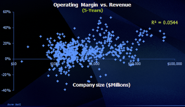
Figure 1: Larger companies are not more profitable over a five-year period than their smaller counterparts
In addition, this wave of consolidation began suddenly in late 2014 after more than 40 years of little or no consolidation (Figure 2). More likely, this new wave of mergers is driven by the low cost of borrowing that facilitates growth of revenue through acquisitions that can easily be accretive to earnings, even if a substantial premium is paid for the acquiree. This merger activity is likely to continue as long as liquidity remains available at low interest rates.
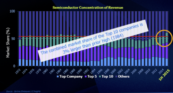
Figure 2: 2015 is the first time in 40 years that consolidation increased in the semiconductor industry
Commoditization of wireless chip sets
Starting two years ago, the pace of withdrawals and acquisitions of companies from the wireless chip set industry has accelerated. As with every major wave of semiconductor application growth (e.g., minicomputers, pocket calculators, personal computers and wireless handsets), there is always consolidation accompanied by price pressures, as growth in unit volumes slows and functions standardize.
Until recently, the emergence and rapid growth of smart phones kept the semiconductor market growing, despite some dramatic changes in leadership among the chip providers. But the growth to enormous volumes of cell phone units, the changes in handset and service provider models (like the Xiaomi low-hardware margin approach) and the relative stabilization of standards has reduced the number of suppliers as well as the chip prices. The same thing happened in the PC industry, as the industry consolidated from more than 100 manufacturers of IBM-compatible PCs. While temporarily painful, those remaining companies become very efficient. And, as always, semiconductor companies can prepare for the next great wave of applications that will drive billion-unit volumes of products that are yet to be identified and developed.
14/16nm brings really new capabilities and challenges
We are accustomed to dealing with new technical challenges with each semiconductor process generation introduced every two to three years. However the basic device structure rarely changes. This year, the industry had to deal with a truly new device structure: the finFET.
The rush to complete the first 14/16nm designs was not driven by cost or complexity, as much as by the need for power reduction that has become the biggest challenge for dealing with the growing complexity of ICs. The finFET change in technology made possible major reductions in leakage, or static power dissipation.
While silicon on insulator (SOI) offered many of the same benefits, its use has been primarily in the design of RF components while, for digital logic, the industry largely chose finFET and then had to deal with the design and manufacturing difficulties. This was further complicated by the fact that extreme ultraviolet (EUV) photolithography has not yet become usable, resulting in the manufacturing and design community adopting techniques for more double patterning.
There have now been sufficient tape-outs that things seem to be stabilizing and the number of 10nm designs is accelerating along with announcement of 7nm availability in 2017.
Since 1973, the primary method of verifying the correctness of the functionality of an IC design has been simulation on general-purpose computers. As chips became more complex, bigger computer server farms were built with tens of thousands of processors used to simulate design functionality. In the 1980s, hardware accelerators were increasingly used to ‘emulate’ the behavior of chips that were so large or complex they did not lend themselves to simulation — such as graphics chips. But the usage remained very limited because emulators were very complex, required numerous connections to peripheral circuitry and were much more laboratory tools than computer servers.
Over the last decade, all of that has changed. The latest generations of emulators have become general-purpose servers that can be placed in a data center like any other server. Even so, the market for emulators has remained relatively flat, at about $160M per year, for ten years. That all changed four years ago and accelerated in 2015. The reason is that complexity of large digital design exceeded the capabilities of simulation on general-purpose computers. Verification of complex microprocessors, networking chips, graphics chips and memory controllers required orders of magnitude more verification than simulation could provide and that started a major transition to hardware acceleration through emulation.
All the major EDA companies competed with custom-designed emulation hardware that offered at least three orders of magnitude faster simulation performance than general-purpose computers. This more than doubled the size of the emulation market over the last three years to an average of about $350M. It also led to the development of integrated simulation/emulation operating systems and design environments. Inevitably, the availability of a ‘virtual’ representation of a chip or system then allowed for verification of the software intended to run on the chip. That is why the emulator has become the hub of a total verification environment that also includes dedicated FPGA cards for additional software verification in many cases.
The second part of this article, where Dr Rhines looks forward to developments we can expect in the year ahead, will be published next Monday, January 11