Accelerate silicon bring-up in a bench-top environment
How a new software-led flow speeds silicon bring-up within the Tessent environment, including a Cypress Semiconductor case study.
The standard silicon bring-up flow is becoming unwieldy, especially for very large designs with complex DFT structures.
After the design, verification, and manufacturing, the first samples are received and the process of silicon bring-up begins to validate that the design performs to specification. As things stand, silicon bring-up involves converting the test patterns to a tester-specific format and generating a test program that is executed by automatic test equipment (ATE). When any pattern fails, the ATE output is translated into chip failure data and processed by diagnosis tools.
But what if you could eliminate the need for expensive tester equipment in the bring-up process, significantly reduce the cycle time, and achieve the same accuracy in diagnosis, using a bench setup and commercial EDA software to run the ATPG patterns? You could expect two key changes: lower silicon bring-up costs and significantly quicker diagnosis of the root cause of test pattern failures.
Mentor Graphics’ Tessent SiliconInsight software enables such a desktop silicon bring-up system.
Silicon bring-up streamlined at the desktop
The Tessent SiliconInsight system (Figure 1) includes a computer connected to a bring-up/validation board with the device under test (DUT). Comparable commercially available setups have until now have been limited to built-in self-test (BIST) and other test instruments accessed exclusively through the DUT’s JTAG port. With this new system, the scope is expanded to non-JTAG test access and a much wider range of pattern applications and diagnosis routines. For instance, ATPG patterns with-chip compression and over 25 external scan channels can be tested and diagnosed at the push of a button.
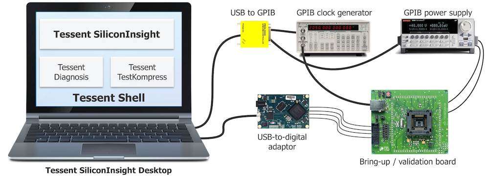
Figure 1. A bench setup for silicon bring-up. A computer running Tessent SiliconInsight, the validation board with USB adaptor, a power supply, and a clock generator (Mentor Graphics)
The key hardware components are a computer, a USB-to-digital adaptor, and a bring-up/validation board with the packaged DUT. The DUT’s I/Os are interfaced with the USB-to-digital adaptor with the help of the validation board. For many designs, such a board is created to facilitate software development and other bring-up applications. The board is typically set up to emulate the conditions present during test on an ATE (such as the power supply pins, clocks, tied pins, etc.), and with all pins required for ATPG available for the USB-to-digital adaptor. Different adaptors can be used, depending on pin count and I/O voltage requirements. Optionally, GPIB-programmable power supplies and clock generators can be used to automate device characterization.
The software that executes the test patterns, and then collects and analyzes the fail data is built on top of the same Tessent Shell platform used to create the test structures and generate the test patterns. This makes it possible for the software to understand how all the test structures and protocols work so that results are returned in a meaningful fashion. When test patterns fail during silicon bring-up, you are typically interested in determining which scan cells capture the failing data. In the presence of on-chip compression and hierarchical DFT, complex decoding and dedicated diagnosis patterns may be required. With this new system, the complex mapping and generation of dedicated diagnosis patterns is now done under the hood, significantly simplifying the debug process.
This bench-top flow (Figure 2) greatly reduces the time for silicon bring-up.
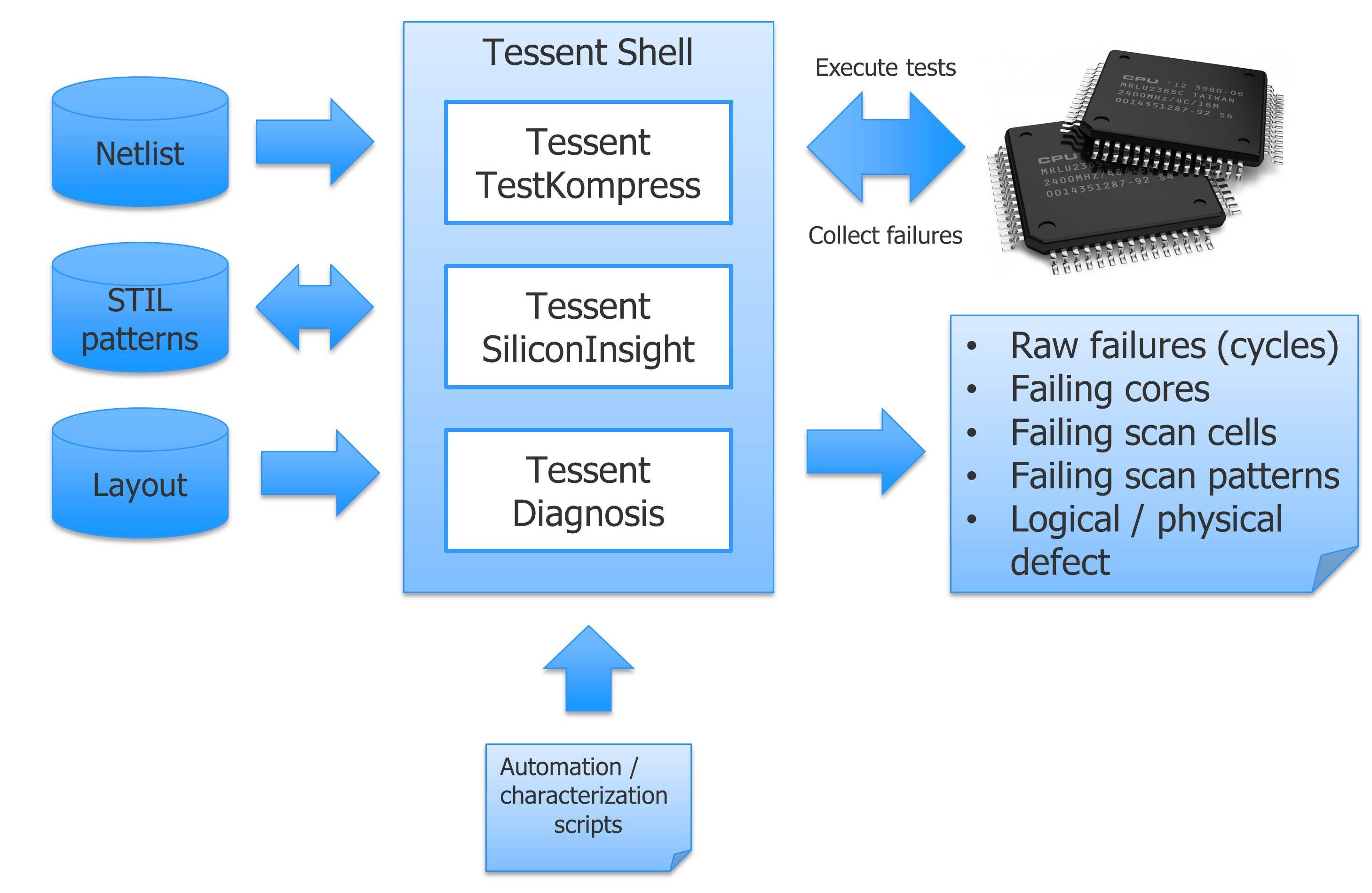
Figure 2. Bench-top silicon bring-up flow (Mentor Graphics)
Cypress Semiconductor silicon bring-up case study
At the 2016 IEEE Workshop on Defects, Adaptive Test, Yield, and Data Analysis (DATA 2016), Cypress Semiconductor described how the system was used to bring up a touchscreen controller chip. The setup is shown in Figure 3. The chip had on-chip EDT scan compression with four scan channels that could be connected toatesterfor theapplicationofcompressedATPGpatterns.
An Opal Kelly XEM6310 USB-to-digital adaptor was connected via USB to a laptop with running Tessent SiliconInsight software. A simple configuration file indicating which adaptor was deployed and the pin map were used to set up the software for this particular DUT.
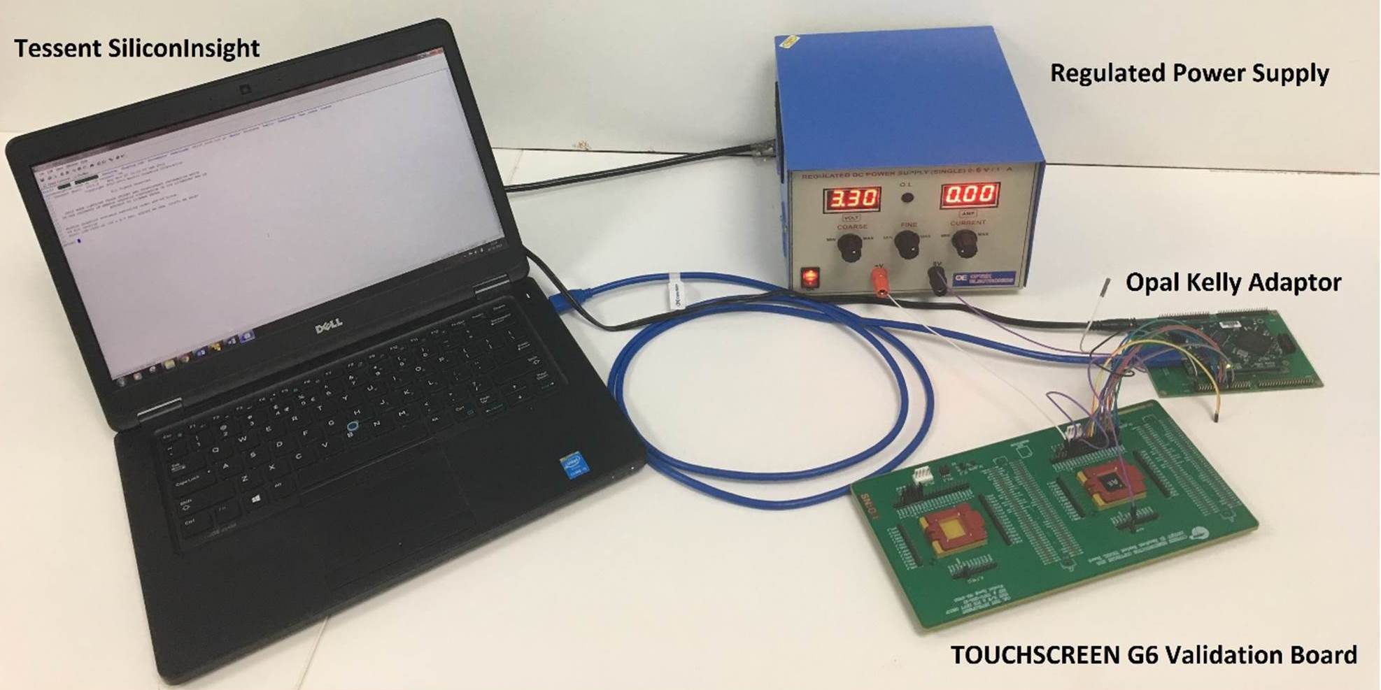
Figure 3. The hardware setup from Cypress’ DATA 2016 presentation (Cypress Semiconductor)
The failing cycle data was automatically collected by the tool during the execution of the ATPG pattern set and used along with the design information todiagnosefailingsuspects.
In this experiment, the results pointed to two failing flops in a scan chain. The user was able to isolate the failing flops and generate a new ATPG pattern set with the faulty chain masked. When this modified pattern set was applied to the DUT, the test passed with no failing cycles.
Further, this flow enabled the user to diagnose the root cause for the silicon failure based on the identified failure location. This could have been done in a conventional bring-up setup, but it would have required a separate test insertion and access to the expensive ATE equipment for silicon bring-up and debug. Using the bench-top flow accelerated the process significantly.
Additional silicon bring-up capabilities
Another feature of the bench-top silicon debug process is that it can include design layout information (in the form of LEF and DEF files). This eases the debug process by locating the fault in the layout. The same methodology can also be used for silicon characterization such as checking the variation in performance depending on clock speed and voltage.
Streamlining silicon bring-up is critical to getting ICs into the hands of customers as soon as possible. Understanding under what conditions an IC fails and effectively isolating the problem helps design, test, and DFT engineers accelerate debug and characterization. This new system increases access to a silicon test and reduces the bring-up root cause cycle time.
About the author
Geir Eide is a product marketing manager at Mentor Graphics.