Efficient IoT system design for AMS, MEMS and photonics designs
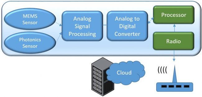
Achieving an IoT design environment that satisfies and supports all facets of system design is a challenge. Using an integrated, top-down design flow that combines analog mixed signal (AMS), digital, RF (radio frequency), photonics, and micro electromechanical systems (MEMS) – enables efficient cost-effective, multi-domain IoT system design (Figure 1). This enables designers to create IoT devices for a wide variety of markets including: automotive, imaging/display, industrial control, medical, sensors, automotive, RF, space, and power management.
Figure 1 A multi-domain system
The design flow can be divided into six domains as follows:
Photonics implementation
Today’s advanced photonics design flow provide significant productivity improvement with a layout-centric design flow. This means that designers can do all of their work directly in the layout editor. When the design is at a point that simulation needs to be run, a netlist can be created directly. This layout-centric design flow removes the need to create a schematic, saving significant time in the design process, as the layout becomes the golden design database. The resulting netlist supports photonic, transistor-level and mixed-mode simulators for designs that have both electrical and optical components. It is extremely helpful if the flow includes formatted PDKs and the industry-standard, interoperable iPDK from multiple photonic foundries. Designers can also create their own components and PDKs.
Analog/mixed-signal implementation
No IoT multi-domain flow is complete without a robust, end-to-end AMS IC design flow. The flow should be optimized for creating custom analog or ‘analog on top’ mixed-signal ICs, working at 28nm and above. An AMS design flow should include highly integrated front- and back-end tools, from schematic capture, through mixed-signal simulation and waveform probing, viewing, and RTL netlist synthesis; to physical layout, place and route, static timing analysis, and foundry-certified physical verification. These tools need to work with all the popular industry tools and industry-standard file formats, as well as providing foundry support.
Digital implementation
Integrated synthesis and place and route engines address the physical implementation of the digital needs of ‘analog on top’ designs. These can help design an analog IC with a small amount of digital control or a more complex mixed-signal IC. They also help with the integration of complex digital circuits with high-performance analog interfaces, providing a complete flow.
Key steps in the flow include:
- Import design data, technology data and specify timing
- Define floorplan and power plan requirements
- Perform static-timing analysis
- Import to layout
RF implementation
Extending mixed-signal simulation to the RF domain provides RF verification for wireless applications in the connected sensor and IoT markets. This requires a set of dedicated algorithms to accurately and efficiently handle the low-power signals in these applications. More advanced tools expand the capabilities of the simulator to provide a wide range of analysis capabilities including a set of RF-dedicated functions, and powerful optimization capabilities for a variety of circuit types.
These algorithms can help designers fine tune circuit performance. The optimization facility does not require any external tools, as it is integrated in the simulation kernel for maximum efficiency.
MEMS implementation
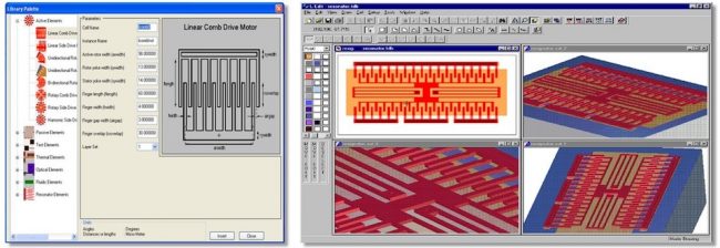
For IoT designs that include MEMS, the multi-domain IoT system design needs to be able to create unique and irregular shapes. Unlike conventional CMOS IC design, which use a Manhattan layout and routing style, MEMS designs use a much broader variety of geometries to suit the needs of mechanical, optical, magnetic, fluidic, and biological applications . The tool shown in Figure 2 provides a unique solution to this problem.
Figure 2 Integrated MEMS design environment
The MEMS solution should include:
- Design tool editor: A central part of the design flow is an advanced layout editor with MEMS-friendly capabilities such as curved polygons and all-angle Boolean operations.
- Advanced design rule checking: This helps designers easily find design flaws and improve yield. A graphical interface for tool setup helps make the tool configurable.
- MEMS 3D modeling: 3D solid modelling allows designers to create a 3D model of a MEMS device from a selected layout area and fabrication process description. The designer can enter fabrication process steps and sequences as well as material properties.
- System-level simulation for MEMS: A compact model builder automatically generates behavioral models ready for system simulation with electronics and packaging, using 3D data from finite-element analysis programs.
Integrating physical verification
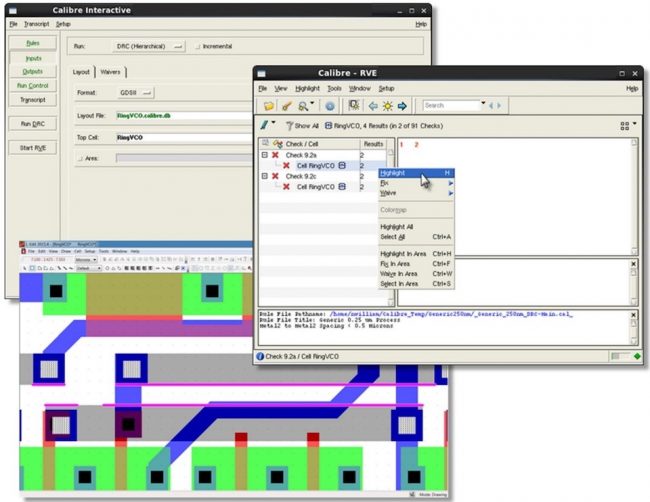
A complete multi-domain, top-down solution needs to span from schematic capture and mixed-signal simulation to full-chip assembly and physical verification. Integrating physical verification into this design flow enables designers to successfully tape out (Figure 3.) the design using the latest technology from the chosen foundry.
Figure 3 Integrated physical verification
Achieving successful tape out
Creating a system that crosses multiple domains is challenging. A multi-domain IoT system design flow enables designers to work in any of the design domains by using flows focused upon the design, simulation, layout, and verification of MEMS, photonics, and AMS elements. This multi-domain approach enables the system’s performance characteristics to be co-optimized to develop a competitive IoT system that provides differentiation in the marketplace.
Further information
To learn more, download our whitepaper, “Implementing a Multi-Domain System”.
Author
Sandra Kupperman is a technical marketing engineer with the Tanner EDA product division of Mentor, a Siemens Business. Sandra is currently the back-end product specialist for L-Edit which is a complete analog/mixed-signal IC physical design environment. She holds a BS in computer science and MS in engineering technology from the University of Central Florida in Orlando, Florida.
Her career in EDA spans 40 years. She was previously employed by Harris Semiconductor, Cadence, Intel, and Synopsys. She has held positions including EDA software developer, CAD engineer, CAD manager, applications engineer, and account manager of technology.
 Sandra Kupperman is a technical marketing engineer with the Tanner EDA product division of Mentor, a Siemens Business.


