Design enablement and entitlement for 14/16nm finFET processes
How EDA tools are evolving to make it possible to design with finFET processes.
FinFET-related processes at 14/16nm and below offer numerous advantages including greater density, lower power consumption and higher performance than previous nodes. The shift from planar to 3D transistors, which enables these advantages, represents a major change whose impact on the design process is being mediated by a set of well thought-through design tools and a strong design ecosystem.
Designers typically have two main considerations as they approach each new process node:
Enablement: are their EDA tools capable of supporting the fundamental requirements to tape-out a chip while meeting all basic requirements such as routing DRC, placement rules, signal EM, etc.
Entitlement: are designers able to cope efficiently with the enablement requirements, the new physics, and generate a design that meets the improved power/performance/area (PPA) projections associated with the process shrink.
The recent shift to 14/16nm processes presents a number of benefits, such as higher performance and lower power consumption, when compared to bulk CMOS transistors. The process changes introduced at the 20nm node, such as new local interconnect structures and advanced lithography techniques such as double patterning, have been enhanced at 14/16nm by the debut of FinFETs; a new device architecture exhibiting desirable electrical characteristics that enables these performance and power benefits.
EDA’s primary role is to accelerate the enablement of 14/16nm finFET processes in a number of ways.
First, it can offer tools for foundries and IDMs, such as TCAD, parasitic extraction and SPICE simulation, which can be used to develop processes that offer the right combination of power, performance and flexibility for the target applications.
Second, but equally important, EDA can provide enhancements to products for design implementation, such as place-and-route, sign-off and IP development, that can help IC designers realize the many benefits of these advanced 14/16nm processes. EDA vendors can also help to ensure that the additional complexities of 14/16nm processes remain manageable for IC designers.
Design advantages and challenges associated with finFETs
The industry has become accustomed to a steady, Moore’s Law improvement in the capabilities of IC processes as it moves to smaller geometries. This improvement began to slacken at the 20nm node, as the leakage from planar transistors at these dimensions became more difficult to control. The introduction of the finFET transistor architecture, which moves the transistor channel out of the bulk into a fin above its surface, has reduced the leakage problem and helped extend the path of Moore’s Law.
- In December 2012, Intel used the International Electron Devices Meeting (IEDM) to outline its 22nm finFET process for systems-on-chip (SoCs) and compare it with its predecessor, a 32nm planar process. Intel said that the low-power variants of the basic finFETs had a drive current 50% greater than the 32nm planar devices.
- In December 2013, again at IEDM, TSMC discussed its 16nm finFET process, and said that the process offered either, a 35% speed gain or, a 55% power reduction, as compared with TSMC’s 28nm HKMG planar process. The 16nm process also has twice the transistor density.
- In March 2014, Tom Quan, director of IP platform marketing, TSMC, opened a panel at SNUG Santa Clara by pointing out that finFETs’ superior IDSat performance, compared to planar equivalents, means higher intrinsic gain – and therefore faster devices for the same power, or lower power for the same speed. He added that the devices also offer better matching than planar equivalents, and exhibit the all-important low leakage, for reducing off-state currents and enabling lower operating voltages.
Taking advantage of the power and performance benefits of finFETs means addressing a number of new design challenges, such as wiring, self-heating and process variability.
Wiring
Wiring is having an increasing impact on the quality of results achievable at advanced process nodes. The cross-sectional area of chip wiring halves (approximately) with each process generation, doubling its resistance per unit length. To address this, IC process developers have built complex metal stacks with wider, lower-resistance wiring on the upper levels.
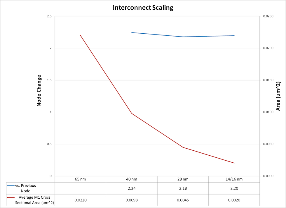
Figure 1 The area of local on-chip wiring approximately halves with each process generation, making wiring resistance increasingly dominant in design (Source: Synopsys)
Place-and-route tools need to intelligently take advantage of these differing wire resistances intrinsic in each layer, allocating routing to the optimal layers to meet timing closure goals.
At the densest wiring layers, complex design rules and the demands of double-patterning lithography mean that place-and-route tools need to make the routing as efficient as possible.
FinFETs are capable of greater drive strengths than planar devices built in the same area, but have two or three times the gate capacitance. The increased drive strength mitigates some of the effects of increasing wiring resistance but with it comes a cost of increased dynamic power consumption due to the increased gate capacitance.
Driving relatively large currents down narrow wires can also create high current densities, which can cause electro-migration (EM) issues.
Careful device optimization by process developers is therefore necessary to achieve the power reduction that a new process node usually promises.
FinFET self-heating
Isolating the channel of the finFET brings advantages in terms of the effectiveness with which the gate can control the current flow through it. Unfortunately, the improved electrical isolation also means greater thermal isolation from the bulk silicon, which can lead to self-heating. This can impact the device’s performance and create reliability issues due to device ageing and negative bias temperature instability.
A self-heating finFET can also heat the overlying wiring, exacerbating EM issues in those nets. Managing this issue demands tools that can provide accurate analysis and efficient remedies.
Process variability
Process variability becomes more difficult to control as device dimensions shrink. In 14/16nm processes, line-edge and width roughness in the process’s densest wiring affects current density, timing and leakage. Increasing RC parasitics and parasitic variability also mean that designers need to create cells and circuits that can cope with such variability. Place-and-route tools must thus be enhanced to minimize parasitics on timing critical nets.
Tool evolution for 14/16nm design success
Design tools are evolving in a number of ways to deal with the new challenges presented by 14/16nm processes.
Place and route
Before each new process node is introduced, there is a large body of work encompassing very tight collaboration with silicon foundries to ensure physical implementation can still achieve three key things.
The first is the basics of enablement to ensure that the foundational basis, including key design rules, are met by the tool.
The second is the best balance of power, performance and area (PPA) in the final design to ensure that the potential advantages of shifting to the new node become a practical reality.
The third is a tight integration with sign-off, so that the implementation process converges on the desired result without surprises.
Enablement for a new node means the ability to produce designs compliant with the necessary placement and routing rules, as previously discussed. However, this is only part of the story. Considerable work is done early in the lifecycle of a technology node to prove out design rules and their implementation, to satisfy process needs while minimizing the impacts on design area, quality of results (QoR), runtime and convergence – in short, the tractability of enablement.
In terms of PPA, the finFET’s device characteristics give the latest process node extra flexibility; designers can choose to use the transistors to achieve better performance at the same operating voltage as an equivalently sized planar device, or to get the same performance at a lower operating voltage. This flexibility gives IC Compiler another degree of freedom as it makes an overall trade-off between timing, leakage and area. But even when timing or performance is a priority, there is still a trade-off to be made with respect to objectives such as leakage and area. IC Compiler’s optimization algorithms have been improved to balance all the design costs to achieve the best result. Since leakage and area vary in a highly non-linear way with respect to timing, this must be done with great care.
Beyond leakage, a larger fraction of overall power is now accounted for by dynamic power. This is influenced by operating voltage and frequency, which are usually defined by the user, and net capacitance. IC Compiler focuses on minimizing overall capacitance to reduce the baseline power consumption. This is achieved by managing placement and routing to reduce overall wire lengths.
IC Compiler incorporates a number of other techniques to reduce dynamic power:
- Low-power placement minimizes the length of very active nets
- Low-power clock-tree synthesis includes careful routing-layer selection and the ability to apply a multi-source approach. This hybrid between a traditional clock tree and a full clock mesh enables the effective distribution of a clock signal at low skew and power
- Advanced clock gating, including the ability to analyze a design’s activity to reveal where a clock signal can be automatically gated
- Automatic banking of single-bit registers into multi-bit cells reduces the area and power used by the registers and reduces the number of points to which a clock signal must be delivered, thereby reducing dynamic power consumption and skew in the clock tree
- Total power optimization, where the vector that includes both leakage and dynamic power is minimized to account for the increased switching power associated with finFETs. This ensures convergence for area and timing goals concurrently with power minimization.
Increasingly, there is also a trend to reduce operating voltage, since it has a quadratic relationship with dynamic power. Here, analysis accuracy – including sign-off correlation for low voltage corners – and optimization effectiveness are key.
Electro-migration (EM) management
With stronger transistors and narrower wires, electro-migration has become an important care-about. IC Compiler’s signal EM capabilities understand the latest foundry rules and are highly correlated to SPICE with sign-off accuracy. This includes temperature-dependent rules, given the thermal dissipation for finFETs. IC Compiler’s EM capabilities can analyze current densities issues for RMS and peak, and can adjust cell and wire sizes to cope with any violations. There are also clock EM prevention capabilities to address both power-rail and clock-signal EM.
Timing closure
To address timing closure, IC Compiler can adjust the placement of integrated clock gates to ensure that timing is balanced between the enable line and the clock. It also has techniques that can concurrently refine both clock and data, in order to meet the design’s slack requirements.
IC Compiler also incorporates techniques to speed up the closure of timing, and to keep timing closed in circuits that may suffer from greater variability than in previous processes. It can find cells that have equal performance in a particular design context. Rather than simply choosing the smallest cell (which may also have the greatest sensitivity to changes in load), it will choose the cell with the least sensitivity. This helps ensure that once timing is closed, it remains closed.
Sign-off integration
IC Compiler is part of the Galaxy Design Platform, a unified solution of best-in-class tools for predictable design closure. Deep integration across tool boundaries enables sign-off integration and accuracy without trading off productivity.
For example, improving the correlation between the implementation flow and sign-off is increasingly important as designs get bigger. It can also help reduce the number of timing ECOs and the time it takes to fix each one.
With Galaxy, this is achieved by using a common signal integrity (SI) model between IC Compiler and PrimeTime SI, with common code for core computations such as cell delay and net delay.
On the extraction side, common extraction modeling between IC Compiler and StarRC sign-off is used, where TLU+ models begin construction with StarRC extraction.
Physical verification
IC Validator has already been used on many 20nm and below tape-outs. It has been updated to handle finFET-specific issues such as verifying fin to fin spacing, fin widths, local layout proximity effects, and source-drain series resistance issues. It has already been proven on finFET tape-outs.
We’ve also made it possible to use IC Validator from within IC Compiler, rather than using it sequentially. It allows physical verification to be tightly coupled to timing, and enables highly effective timing-driven metal fill. This reduces the likelihood of multiple iterative cycles. This In-Design capability also extends to integrated power analysis using PrimeRail, which can expose EM issues, power-density hot spots and potential dynamic voltage drops on supply rails.
Conclusions
FinFET-based processes bring strong design advantages and a set of new design challenges. Some of these can be made transparent to the IC designer through careful process and process-rule development, or encapsulation in cell libraries or tool algorithms. Others must be managed directly, ideally with support from design tools. Synopsys’ tool enhancements to support 14/16nm design focus on two things: ensuring that shifting to the new node will result in designs with the right combination of power, performance and area; and ensuring that, due to tight integration with the sign-off process, design implementation can proceed without any unpleasant surprises.
Author
Dr Henry Sheng is senior director of R&D for digital physical design at Synopsys. He is responsible for silicon enablement technology, including routing, extraction, timing, signal integrity and electro-migration. He has a PhD in electrical engineering and computer science from UC Berkeley.
