Why comprehensive memory layout verification needs automated reliability checks
Because of the high analog content in memory designs, designers must understand how various effects impact reliability and performance.
Memory chips are essential for data storage in most system-on-chip (SoC) designs, low-power applications, and general-purpose processors. Accurate, consistent memory performance is essential to the operational fidelity of these applications. Ensuring the operational reliability of memory structures requires comprehensive reliability verification for both front-end (circuit) and back-end (physical/geometrical) memory designs. However, memory design contains a substantial amount of analog circuitry, so it is critical that designers understand the design and manufacturing conditions that can affect analog performance and reliability, and how reliability verification can be used to find and mitigate their effects.
Why automate analog circuit reliability verification?
Historically, designers have visually reviewed an analog layout with the layout engineer to find any areas that do not comply with the design constraints. However, for complex memory designs and advanced nodes, manual inspection has become more difficult, more time-consuming, and more prone to human error. Additionally, designers should re-check the design after each design change, no matter how minor. This step is often skipped because of time and resource constraints, which can result in small discrepancies that may not be caught by post-layout simulations.
For example, memory systems contain essential analog circuits. These include devices like sense amplifiers (SAs) that read and amplify the data signals from the memory cell. SAs are one of the critical differential analog components of dynamic random-access memory (DRAM) [1,2]. Analog circuits like SAs are typically extremely sensitive to changes in layout design technique, operating conditions, and process variation. Designers who want to achieve DRAM design targets must focus on the operational reliability of SAs, using multiple reliability verification strategies to ensure their designs will provide the intended performance and be resistant to manufacturing variation.
Verifying physical layouts also has a direct impact on analog design reliability and performance. Layout-dependent effects (LDEs) and impacts from manufacturing or operational variation can render a chip useless in production. While analog design schematics usually match the expected performance accurately, it is not uncommon after physical implementation is complete for a layout to contain discrepancies between the schematic and physical layout that affect the final quality. Layout constraint checking is used to find these inconsistencies so that designers can eliminate or mitigate potential performance and reliability issues during the design phase, before the design is taped out.
In addition to the physical layout verification, topology checking is essential to verify a range of critical design impacts. Checks here include counting device types, verifying existing device models in the design, or calculating the average device properties (e.g., width, or number of fingers).
All these requirements and concerns drive the need for an automated reliability verification process that can provide accurate, consistent results in a timely manner across all designs and process nodes. Let’s take a closer look at some specific reliability issues in analog design.
Analog design reliability and performance
Impact of layout implementation
The performance and reliability of analog designs are closely linked to the layout implementation. Once the physical layout of an analog design is complete, and circuit implementation has been validated with layout vs. schematic (LVS) verification, the layout must be analyzed for many potential LDEs that can impact reliability and performance. While some can be caught during post-layout simulation, others will not be seen until the design is on silicon, so finding and eliminating them during design verification is essential to success.
There are two significant LDEs that affect analog design reliability and product lifetime: well proximity effect (WPE), and shallow trench isolation (STI) stress. Both WPE and STI stress have a negative impact on transistor electrical parameters (e.g., threshold voltage), and thus on transistor performances [3,4]. These LDEs can change the circuit behavior even when the schematic simulation is accurate.
WPE is created by the distance between devices and the edge of the well in which they are placed. For symmetrical aging, all devices in a well must have the same spacing to the edge of the well. Devices with even a small difference in the distance between the device and the well edge will age differently, which can lead to performance degradation, and eventually reduced product life. Figure 1 shows a layout where multiple devices in the well do not have the same spacing distance to the well edge, which will create the WPE.

Figure 1. WPE leads to differences in device aging, which contribute to performance degradation over time (Siemens EDA)
STI, on the other hand, is deliberately created during manufacturing to enable closer spacing of transistors while preventing current leakage between them. However, creating STI also creates new stresses. To ensure identical STI stress parameters, the shapes (polygons that define the device) of all the devices belonging to one group must be symmetrical. Moreover, the shapes surrounding these devices within a certain distance (the context layer) should also be the same. This uniformity ensures that not only will STI stress be the same for all the devices within the same group, but also that all the coupling will be the same (e.g., the same metal1 area on top of all the devices).
Impact of manufacturing and operational variations
Once a design is sent to manufacturing, it will experience the normal and unavoidable variation found in any manufacturing process. There are two significant variation effects related to manufacturing: metallization process variation and thermal/process variation. Unfortunately, these variations cannot be anticipated since the manufacturing process is never perfectly repeatable.
In addition, when the final product is placed in operation, the conditions under which it operates can greatly affect performance and product life. Most designers have no information about the operating environment in which the final chip will be used.
Anticipating and minimizing the impact of manufacturing variation effects requires an understanding of the underlying causes, and how proper design and verification can improve the ability of a design to withstand these inevitable variations.
Improving analog reliability through design and verification
Physical design and verification
Over the years, analog designers have developed number of best practices to minimize the creation and impact of WPE and STI effects. These include:
- Symmetry between devices;
- Current orientation matching;
- Dummy device insertions;
- Common centroid between devices;
- Same pitch between devices; and
- Electrical parameters matching
To fully validate analog layout reliability, designers must typically run multiple checks that cover these and related layout issues.
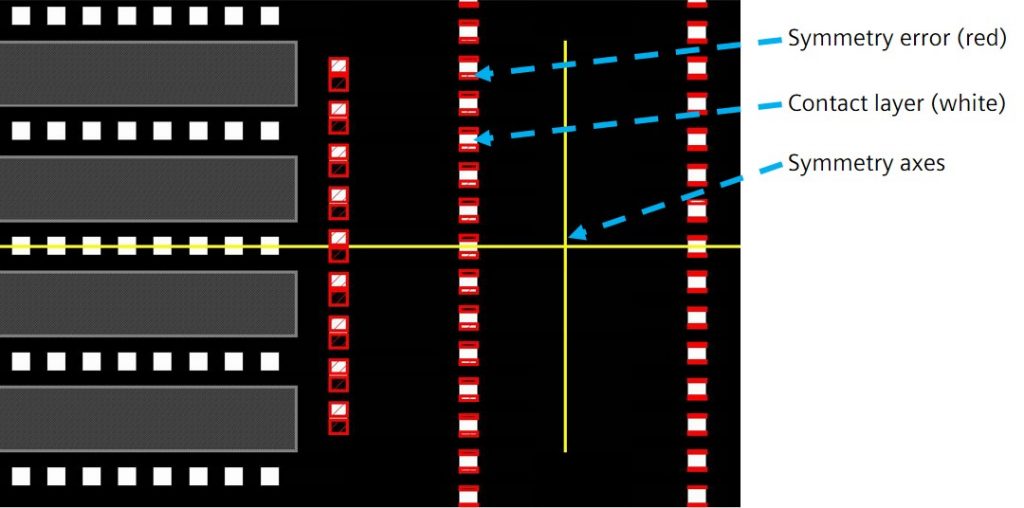
For example, a symmetry check between devices ensures all the devices have symmetrical shapes around either horizontal/vertical axes, or around the center. For an array of devices, checking for device shape matching and identical pitch between all devices ensures the uniformity of the array. Figure 2 shows an example of a symmetry mismatch.

Figure 2. Symmetry mismatch for a group of devices reported by an analog layout reliability check (Siemens EDA)
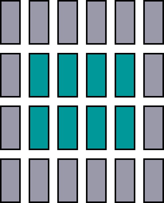
Adding dummy devices around a group (array) of devices is a design strategy used to reduce the impact of both WPE and STI stress for the array by standardizing the distance between the active devices and the well edge, increasing the uniformity of the WPE and STI stress experienced by the active devices (Figure 3). An automated constraint checking tool can check for the presence of these dummy devices.

Figure 3. The use of dummy devices (grey) placed around an array of active devices (green) to standardize spacing in an array configuration (Siemens EDA)
Similar to WPE and STI stress, one way to minimize the effect of manufacturing variation is to ensure consistency in device design. Common centroid design implements schematic devices as multiple layout devices with a common center. This helps mitigate variation effects on each schematic device by ensuring that each device is affected in a similar manner. In common centroid checking, the center of each device is determined (Figure 4). If those centers have the same location (x/y coordinates), then the devices have common centers and will experience the same average variations.

Figure 4: An array of devices where the three source devices (A, B and C) are symmetrical with respect to a common center (Siemens EDA)
Topological design and verification
In today’s complex designs, topological reliability often requires integration across physical devices and circuit design. Topological checks are used throughout the design flow to validate both full chip and intellectual property (IP) designs. Typical topological reliability checks perform a variety of actions. These include:
- Count devices per device type and subtype.
- Count devices that have device properties valid within a defined constraint (e.g., length > specific threshold).
- Obtain average device properties, such as width, length, or number of fins.
- Identify any unexpected device type or subtype in the full chip (this check is critical if some specific device types or subtypes are not permitted in the design).
Automated layout reliability verification
Some EDA [5] constraint checking tools can automatically and accurately detect subtle reliability errors using a variety of both topology checks and analog layout constraint checks. These include device symmetry, device orientation, the presence/absence of dummy devices, and common centroid layout accuracy [6,7].
The biggest advantage of automated constraint checking is that it is deterministic, meaning that the result of an automated check will always be the same for a given set of inputs. This eliminates the chance of human error. In addition, automated reliability verification is typically faster than detailed manual inspection, but still ensures that all desired and required checks are performed.
In an automated analog constraint verification flow, the designer determines which devices must be checked, and which check(s) should be applied to each group of devices. The constraint checking tool can then automatically check each group of devices and report any violations.
A thorough discussion of the need for symmetry checks in layout reliability verification is discussed in [8], while a review of automated checks for analog constraint checking is available in [9].
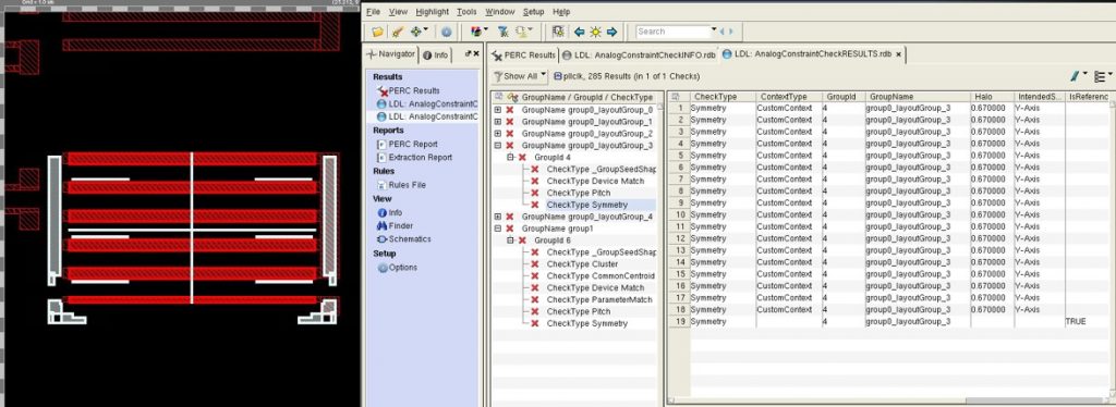
The Calibre PERC reliability platform from Siemens EDA is a full-featured reliability verification tool that makes it easier for design teams to perform comprehensive reliability verification by providing pre-coded checks that automatically analyze and validate a wide variety of reliability design issues. Designers can select and combine these checks as needed to ensure full reliability verification coverage for each layout. Figure 5 shows the results of a Calibre PERC flow. Designers can debug these results (as error or informational results) using the Calibre RVE results viewer.

Figure 5. A snapshot showing results for symmetry, device matching, and common centroid checks from the Calibre PERC reliability platform (Siemens EDA – click to enlarge)
Conclusion
Memory circuits are critical for many applications, but the need for consistent and precise memory performance places a heightened focus on reliability. Accurate and full verification coverage of multiple reliability concerns is essential. Because of the high percentage of analog content in memory designs, designers must have a thorough understanding of how design, manufacturing, and operational effects can impact memory reliability and performance. This knowledge enables them to accurately analyze and optimize their designs to ensure they meet design reliability goals.
An automated reliability verification platform should enable designers to quickly and easily select, configure, and combine multiple checks to ensure full and accurate reliability verification in a timely manner. These reliability checks analyze the circuit layout to highlight symmetry, device matching, or common centroid issues that may impact memory performance or result in operational failures. Error results should assist designers in fast and accurate debugging and correction. Tools like the Calibre PERC reliability platform enhance ease of use by providing many checks as pre-coded checks that can be quickly selected and combined as needed. Because designers can use the Calibre PERC packaged checks flow to select and combine checks without the limitations of check coding or complex setup, running reliability verification is easier, faster, and more consistent, which helps shorten the design time cycle while safeguarding product reliability.
References
[1] J. V. Faricelli, “Layout-dependent proximity effects in deep nanoscale CMOS,” in Custom Integrated Circuits Conference (CICC), 2010 IEEE, IEEE, 2010, pp. 1-8. DOI: 10.1109/CICC.2010.5617407 URL: https://ieeexplore.ieee.org/document/5617407
[2] C.-W. Lin, J.-M. Lin, Y.-C. Chiu, C.-P. Huang, and S.-J. Chang, “Common-centroid capacitor placement considering systematic and random mismatches in analog integrated circuits,” in Design Automation Conference (DAC), 2011 48th ACM/EDAC/IEEE, IEEE, 2011, pp. 528-533.
URL: https://ieeexplore.ieee.org/document/5981853
[3] P. G. Drennan, M. L. Kniffin and D. R. Locascio, “Implications of Proximity Effects for Analog Design,” IEEE Custom Integrated Circuits Conference 2006, San Jose, CA, 2006, pp. 169-176.
DOI: 10.1109/CICC.2006.320869
URL: http://ieeexplore.ieee.org/stamp/stamp.jsp?tp=&arnumber=4114933&isnumber=4114894
[4] Wu, Po-Hsun, et al. “Common-centroid FinFET placement considering the impact of gate misalignment.” Proceedings of the 2015 Symposium on International Symposium on Physical Design. ACM, 2015.
[5] Siemens Digital Industries Software. “Calibre PERC reliability verification solution.” https://eda.sw.siemens.com/en-US/ic/calibre-design/reliability-verification
https://resources.sw.siemens.com/en-US/fact-sheet-calibre-perc
[6] Hossam Sarhan, “Comprehensive layout reliability verification for memory design,” Siemens Digital Industries Software.
https://resources.sw.siemens.com/en-US/white-paper-comprehensive-layout-reliability-verification-for-memory-design
[7] Hossam Sarhan, “Configurable, easy-to-use, packaged reliability checks,” Siemens Digital Industries Software.
https://resources.sw.siemens.com/en-US/white-paper-configurable-easy-to-use-packaged-reliability-checks
[8] Sherif Hany, “Advanced symmetry checking in IC layout design and verification”, Siemens Digital Industries Software.
https://resources.sw.siemens.com/en-US/white-paper-advanced-symmetry-checking-in-ic-layout-design-and-verification
[9] Hossam Sarhan and Alexandre Arriordaz, “Automated Constraint Checks Enhance Analog Designs Reliability”, Siemens Digital Industries Software.
https://resources.sw.siemens.com/en-US/white-paper-automated-constraint-checks-enhance-analog-design-reliability
About the author
Hossam Sarhan is a senior product engineer in the Design to Silicon division of Siemens Digital Industries Software, supporting the Calibre PERC reliability platform and Calibre PEX tools. His current work focuses on circuit reliability verification and inductance parasitics extraction. Prior to joining Siemens, he worked in modeling and design optimization for on-chip power management circuits. Hossam received his B.Sc. from Alexandria University, Egypt, his M.Sc. degree from Nile University, Egypt, and his Ph.D. from CEA-LETI, Grenoble, France.