Placement optimizations push power and clock on Cortex-M7 project
Soft blocking to prevent cell spreading and other placement-optimization techniques helped improve power and clock speed on a Cortex-M7 test chip designed by ARM and Cadence.
ARM’s Cortex-M7 was quickly snapped up by partners as a high-speed microcontroller that can take on some safety-critical tasks. At ARM TechCon, Paddy Mamtora, product engineering and group director at Cadence Design Systems explained how, with ARM, a team approached the problem of “pushing performance and at the same time pushing power”.
Mamtora explained the project for the M7 test chip was the latest in a series of designs that started with a Cortex-A15 device in 2010.
“We were the first to come out with A15 on 20nm. These designs are done early in the timeline. The goal is to not to push for PPA but to make sure that the process flow has been flushed,” Mamtora said. This project was different in that it was intended to push performance further than usual for a test-chip design.
“The M7 leads to two times the DSP performance over the M4,” said Mamtora. “But there are PPA and timing closure challenges. There are complex datapath structures. There are a number of high-fanout signals that need optimal placement because of the superscalar nature of the M7. And it needs critical I/O timing that puts extra pressure on register-register data paths.
Image Soft-blocked floorplan for the Cortex-M7 project
“You need high performance in terms of frequency but you also need handles in the flow to recover power. The process has reduced leakage so our main focus was on dynamic power. The other thing we tried to explore was that, yes, we are trying to push frequency with optimal power. We also care about people who don’t want the highest frequency but they want the lowest power at not such a high frequency. The question we asked ourselves: do we need two different recipes?”
The design was targeted at TSMC’s 40LP process – because it will soon have embedded-flash support – with a single Vt using both the core and physical IP from ARM.
Single-Vt implementation
“We used a single Vt because we were very conscious of existing leakage reduction and methods. We wanted to focus on leakage reduction from the flow not the technology. This flow is independent of what process you use,” said Mamtora.
For implementation, the team employed a flow based on RTL Compiler and the Encounter Digital Implementation System. “Stepwise the flow was no different to normal. What was different was the focus points,” said Mamtora.
Mamtora noted that capacitance and gate capacitance are the key factors that dominate dynamic power today. But the floorplan size was bigger than required for the design, which would tend to lead to the design tools, to avoid congestion, spreading cells out uniformly and causing longer wire and clock delays than would be the case in a tighter placement. To prevent more critical cells from being spread out, the team placed soft blockages to increase placement density to above 75 per cent.
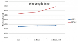
Image Reduction in wire length thanks to timing-driven optimizations
Mamtora said the team also took of the latest version of the Giga Place placement engine to focus on wirelength adjustments within critical groups of cells. “Previously placement was not necessarily aware of timing as primary function. It was mainly based on wire length using bounding-box algorithms. But sometimes when you are timing driven you can’t use that as your drive component. So with Giga Place we can use slack as a forcing function.”
Another issue that becomes apparent on denser nodes is pin access. Even with a sparse placement it is possible that the router lacks the ability to route from pin to pin because of design rule conflicts. “So Giga Place has added pin access algorithms,” Mamtora said, pointing out there are further changes to support routing at the placement stage.
“Giga Place starts in an electrically driven mode, which gives you the shortest delay but not necessarily the shortest path,” Mamtora added. The use of “in-route optimization” with the placement engine uses timing and signal-integrity estimation algorithms to make placement changes before committing to a final detail route.
Avoiding over-constraints
“If you are not signal-integrity aware you tighten a lot of constraints up front. Then you find that if you want to increase frequency you can’t do it. It uses an internal extraction engine, which offers far more effective RC modeling than before and reduces over-constraints.”
Mamtora said the tool can do both back end and front end optimizations and performs tasks such as leakage power reduction: “All the power transforms are becoming leakage aware.”
Compared to a flow based on the 13.2 EDI release, the 14.1 release with the optimizations achieved a 4 per cent improvement in microwatts per megahertz at a target of 400MHz. The use of dynamic power optimizations such as activity aware synthesis and placement achieved 9 per cent less power over 13.1. Allowing the peak clock rate to fall to 200MHz saved 25 per cent over the 400MHz design on release 13.1. Adding dynamic power optimizations, using Giga Place enhancements and relaxing the clock skew led to a 38 per cent cut in power versus the original 400MHz, release 13.2 implementation.
Cadence covers more details in a white paper that looks at the use of Giga Place and EDI on Cortex-M class designs.

