Multi-corner multi-mode signal integrity optimization
Signal integrity (SI) is an ever-growing problem as more interconnect effects and fast clocks increase the chances of crosstalk noise and glitches as well as unexpected signal delays. There has been a significant increase in SI-related timing violations due to the increasing influence of lateral wire capacitance in designs at 65 and 45nm. A fast-increasing number of operational modes and process corners in which a design must operate is exacerbating the problem and significantly increasing the time needed to reach design closure.
To properly address SI closure for ICs manufactured at 65nm and below, we need to take SI into account throughout the design flow. It must be on the agenda from the start of placement, and stay on it through clock tree synthesis, optimization and routing. We must be equipped to undertake accurate analysis, and to apply effective prevention and design optimization techniques at all appropriate stages.
Additionally, we need the ability to perform concurrent SI analysis and optimization for all operational modes and process corners. This requires a new place-and-route architecture that has an underlying ability to carry out multi-corner multi-mode (MCMM) timing analysis. Solutions without true MCMM capability can only present a single mode/corner combination for SI analysis at any one time, forcing design teams to run multiple time-consuming iterations of the tool and also to intervene manually in the process.
Signal integrity (SI) refers to the degree of immunity a design has to crosstalk effects caused by parasitic capacitance between adjacent nets. Cross-coupling can cause changes in signal slew rates and delays that affect timing closure, and also signal glitches that can induce logic errors. SI analysis uses specific terminology to refer to the two kinds of nets it considers:
- The ‘victim net’ is the net being analyzed for crosstalk effects.
- The ‘aggressor nets’ are all the surrounding nets that could contribute to crosstalk in the victim net.
The goal of SI analysis is to calculate the ‘voltage bumps’ that can be induced in the victim net due to the coupling of signals from the aggressor nets. These will be dependent on both the size of parasitic elements (conductor resistance and inter-conductor capacitance) and the relative timing of the signals on victim and aggressor nets. Signal alignment will determine the amount of reinforcement or cancellation that occurs among signals.

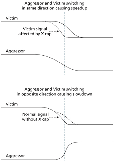
Figure 1. Effects of crosstalk on victim signal transition. Source: Mentor Graphics
Figure 1 shows how aggressors transitioning at the same time and in the same direction as the victim reduce the victim signal’s arrival time (reducing timing delay), while aggressors transitioning opposite to the victim will cause its arrival time to increase (increased timing delay). Determining these changes in victim transition times is called ‘delta-delay’ analysis and forms an important subset of SI analysis.
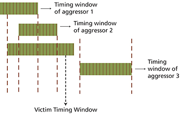
To take the effect of timing into consideration, SI analysis uses the ‘timing window’ concept. A timing window is the difference between the late and early arrival times for a signal at a node, and it is attributable to different paths through the nets. A voltage bump will only have an effect on operation if the timing windows of the aggressor and victim overlap (Figure 2).
SI challenges at advanced process nodes
There is a group of factors that arise or become more significant at 65nm and below in accounting for much of the greater difficulty in achieving SI closure:
- Interconnect coupling capacitance increases.
- Wire resistance and variations in resistance also continue to increase.
- Clock timing gets faster. There are then several key challenges to performing effective SI analysis for ICs at advanced process nodes:
- A need to analyze many more modes and corners than for previous generations makes it harder to reach timing closure.
- Smaller geometries mean SI effects are more pronounced and cannot be prevented—let alone optimized—by avoidance heuristics alone. Real-time analysis and feedback during the routing process are now required.
- Designs with huge gate counts require extremely fast and efficient SI analysis and optimization or turnaround times can become excessive.

Figure 2. Using timing windows to determine the impact of crosstalk. Source: Mentor Graphics
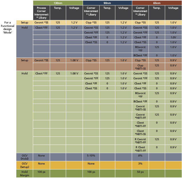
The soaring numbers of process corners and operational modes have augmented the SI closure problems at deep submicron geometries, and each new node brings with it further increases in both. A 130nm design typically has four process corners to consider for each given operational mode (e.g., functional or test modes). At 65nm, there are typically 21 corners for each mode (Figure 3). Additional operational modes, particularly those used to control power consumption, add exponentially to the design’s variation complexity.
Parasitics vary for each process corner to be considered, and timing calculations vary for each IC operational mode and process corner. This means that there are different sets of arrival times (i.e., timing windows) for each mode and corner combination. Traditionally, timing analysis tools can handle just one case at a time because they track only a single timing window for each node in the circuit.
Clock trees and signal integrity
Many techniques used to control power consumption in clock trees are also inherently beneficial for achieving SI closure. Clock tree synthesis requires the robust implementation of length control rules, clock gating and load balancing. In clock tree routing, clock wires should be shielded to reduce coupling capacitance between active clock wires and neighboring nets. Typically, clock nets are routed with non-default rules (NDRs), which are either defined in the technology files or specified by the user before clock routing. The NDRs for clock routing usually define double-width wires and double spacing around wires as compared to the default rules. Double-width wires reduce wire resistance, and double spacing allows room for shielding to be added. Shielding is simply grounded metal that dampens any signal noise from the active clock nets.
Traditional place-and-route systems fail on SI closure
The main place-and-route (P&R) tools in the market are typically 10-15 years old and were originally architected to address a different set of problems. They are no longer adequate for reaching design closure on timing, SI and power constraints within tight design schedules at today’s geometries.

Figure 3. Growing number of process corners to consider. Source: Mentor Graphics
Most P&R tools have a ‘timing graph’—the most fundamental data structure in any implementation system—that was built to handle analysis across one mode and one setup/hold corner at a time. All P&R engines, including those for timing analysis, are limited by the information stored in this data structure. As it is very difficult to replace or retrofit this basic architectural limitation, it is nearly impossible for traditional P&R software to efficiently address MCMM design closure.
The inability to perform truly concurrent MCMM timing analysis forces designers to deal with modes and corners by doing separate extractions for each process corner, and launching separate SI analysis runs for each mode/corner combination. The results must then be manually combined and analyzed using custom scripts and other ad hoc techniques to achieve closure. This can lead to time-consuming iterations needed to fix SI problems found after routing. Unfortunately, there is no way to have confidence that the design is really optimized for all modes and corners with this approach. That is, there is no real SI design closure.
MCMM timing improves SI closure
We need an architecture that can comprehensively address the variability problem throughout the design flow. It must remove unpredictability from the physical implementation process and help designers stay on schedule, while tackling the advanced design challenges of 45nm and below. An effective P&R solution delivers a comprehensive set of capabilities to help designers close timing, power and SI across any number of modes and corners. Some of the features needed in such a tool include:
- a timing analysis architecture that concurrently addresses multiple modes and corners;
- a variability-aware routing approach that optimizes for lithography, critical area analysis and other design for manufacturing metrics during P&R;
- a flexible tool architecture and power reduction technologies that address the full spectrum of low power design styles; and
- a scalable data model that can represent 100+ million gate designs in hierarchical or flat design methodologies.

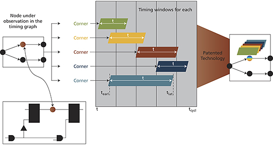
Figure 4.The Mentor Graphics Olympus-SoC MCMM P&R System. Source: Mentor Graphics
Designers need a P&R architecture that can maintain any number of timing windows per node, even for the largest IC designs. This is where MCMM timing analysis reveals itself as an effective way of computing timing windows concurrently across all modes and corners in a single pass. This kind of functionality is available in the Mentor Graphics Olympus-SoC MCMM P&R System (Figure 4).
For SI analysis, this means that victim and aggressor timing windows for all modes and corners are considered concurrently, rather than one at a time. MCMM-SI analysis addresses reliability issues such as crosstalk delay, glitch, power and electromigration while reducing the time to design closure. In addition, detailed routing and optimization engines also address SI violations concurrently over all variation scenarios.
With a true MCMM analysis capability, designers are freed from a time-consuming iterative SI closure process and are assured that new violations have not been introduced by SI modifications. Designers can tape out much more quickly with a higher confidence that the design meets all SI as well as other closure requirements.
Additional P&R strategies for SI closure
MCMM timing capability is the most fundamental difference between recently architected tools and the incumbent P&R solutions, but there are additional strategies that deliver further SI efficiencies during physical implementation. These include:
- SI-aware placement that attempts to minimize parallel wire lengths;
- MCMM clock tree synthesis;
- the automatic shielding of clock nets;
- logical SI optimization (sizing, buffering, white space optimization);
- crosstalk prevention techniques such as SI-driven track assignment, wire spreading and track reordering;
- implicit shielding, whereby route nets active in different modes are placed together as neighbors;
- fast, incremental SI updates over all mode/corners concurrently (this enables signoff-quality SI optimization throughout the routing and post-route flow, a correct-by-construction approach called ‘SI-driven routing’);
- very fast, multi-corner extraction on-the-fly, providing parasitic information for all modes and corners to enable SI-driven routing;
- the ability to deal with multiple voltage islands; and
- post-route optimizations for SI that include cell-based optimizations, slew balancing and slack improvement.
Conclusion
Increased SI effects, more manufacturing variability and burgeoning gate counts all challenge traditional P&R tool architectures. To ensure SI closure success at 65nm and below, designers need a high-performance P&R system that addresses the specific difficulties arising at today’s advanced process nodes. The key technological requirement is a signoff-quality MCMM timing engine that computes delay shift and glitch for any number of mode and corner scenarios in a single pass, eliminating SI violations over all variation scenarios concurrently.
Mentor Graphics
Corporate Office
8005 SW Boeckman Rd
Wilsonville
OR 97070
USA
T: +1 800 547 3000
W: www.mentor.com