How to gain a competitive edge with advanced DFT
For any new SoC project, more things can (and often will) go wrong than are ever imagined during the optimistic early phases of product definition. However, the semiconductor industry continues to deliver incredible advances in IC capabilities. The most successful companies continually refine and optimize all aspects of design and fabrication, including the increasingly important stage of design-for-test (DFT).
DFT ranges from the insertion and verification of test logic at the RTL all the way through to the failure analysis of failed fabricated devices. Advanced DFT strategies not only ensure that a device meets quality and reliability requirements, but also help improve yield, reduce costs, and get products to market faster. So what are the elements of an advanced, smart DFT strategy? How do you go beyond finding a solution that does little more than the basic purpose of DFT (detecting manufacturing defects)?
Research and development in DFT has been lively and productive for several decades. Breakthroughs such as embedded deterministic test (EDT) and others have prevented test costs from overtaking budgets and helped to improve the test quality of ICs across the board.
Let’s look at some of the most significant areas of DFT R&D that have delivered solutions for today’s most challenging designs, such as extremely large artificial intelligence (AI) processors that require hierarchical plug-and-play methodologies, and automotive SoCs that must satisfy very high manufacturing test standards and have extensive in-system test capabilities.
Better defect detection
First, DFT must catch defects in manufactured silicon and ensure that a part will operate correctly once it is placed in-system. We can make basic predictions about the expected defect level depending on the process yield. But if your fault coverage is too low, you ship bad parts and your business suffers. And what is ‘too low’? Well, for ICs in automotive safety systems, 99% is too low.
For any IC in a safety-critical role, the fault coverage needs to be much higher than normal. This requires the use of cell-aware fault models that can target potential defects within the technology cells. Major semiconductor companies, including AMD (Hapke, 2014), have seen dramatic improvements in fault coverage using this technique.
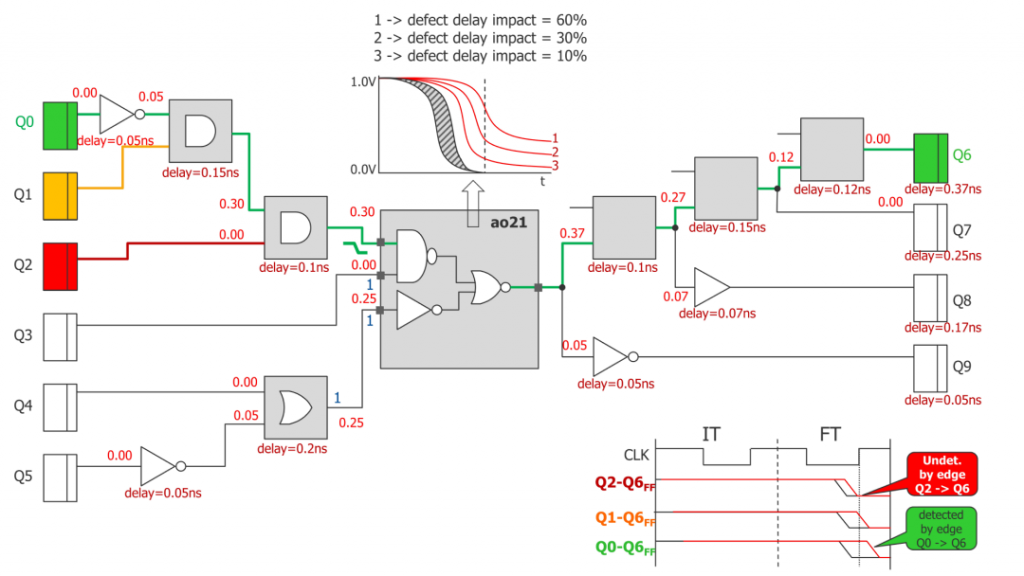
Indeed, cell-aware test and advanced fault models have been expanded to include new types of bridge, opens, cell-aware/timing-aware (Figure 1), and cell-neighborhood tests. This so-called ‘automotive-grade’ test has been further vetted by companies such as Intel and ON Semiconductor, who have subsequently published their research.

Figure 1. Timing-aware ATPG combined with cell-aware test finds small delays considering the longest paths and delays within cells (Mentor – click to enlarge)
Scan test is just one part of DFT. Built-in-self-test (BIST) is a necessary companion in many of today’s designs. Memory BIST detects failures in embedded memories and their interface logic. It needs to manage designs with a huge number of memory instances. This requires a DFT tool that works efficiently in a hierarchical DFT methodology. Hierarchical DFT for designs of this scale requires fully automated solutions that can work with higher-level user input across all parameters (test time, area consumption, power consumption, etc.)
Numerous case studies have been published that show the benefits of hierarchical DFT. It generates patterns at the block level and directly reuses those patterns at the top level. Some of its main benefits include:
- A 10X performance gain in ATPG, diagnosis, and pattern verification;
- An up to 2x reduction in pattern count;
- The removal of DFT from the critical path; and
- The enabling of core re-use.
Detecting more faults usually requires larger sets of test patterns, which increases demand on compute resources, test time and cost. There are several strategies for managing higher test volumes. One is to use hierarchical DFT.
A new kind of test point was recently introduced that dramatically reduces pattern size. Companies like Broadcom (Konuk, 2015) have used this kind of point to control the growing test pattern counts. An even newer technology for logic BIST, called LBIST Observation Scan Technology, has been introduced specifically to improve in-system test speed for automotive devices.
Improved yield
DFT doesn’t end with detecting manufacturing defects. It also helps to improve the manufacturing process and increase yield, with a direct impact on business. Manufacturing test collects massive amounts of data from failing tests, and these can reveal valuable information about the mechanisms that cause a circuit to fail. This data needs to be analyzed through scan diagnosis to detect the true causes and locations of circuit failures. Scan diagnosis improves the success of physical failure analysis used to validate the defect mechanism. Advanced scan diagnosis has been used by foundries like GLOBALFOUNDRIES so that they can more efficiently find the root causes of failures (Benware, 2012).
Fixing a systematic yield problem requires data about the failure mechanisms on a whole population of failing die across wafers and lots. Performing volume scan diagnosis, an advanced technique that uses statistics and machine learning, speeds yield ramp for new processes and improves yield for mature processes. This technology is in use in many successful companies.
Streamlined DFT flow
All the DFT technologies available today will fail to enhance your competitiveness if they are difficult to integrate into reliable design flows. Introducing a hierarchical DFT flow is probably the biggest single change you can make to reduce your overall DFT implementation effort. The technique has already been widely adopted, and leading players such as Amazon (Trock, 2016) and Samsung (Shin, European Test Symposium/IEEE Embedded Workshop 2019) have both published accounts of dramatic improvements they have seen across all aspects of DFT by adopting hierarchical methodologies.
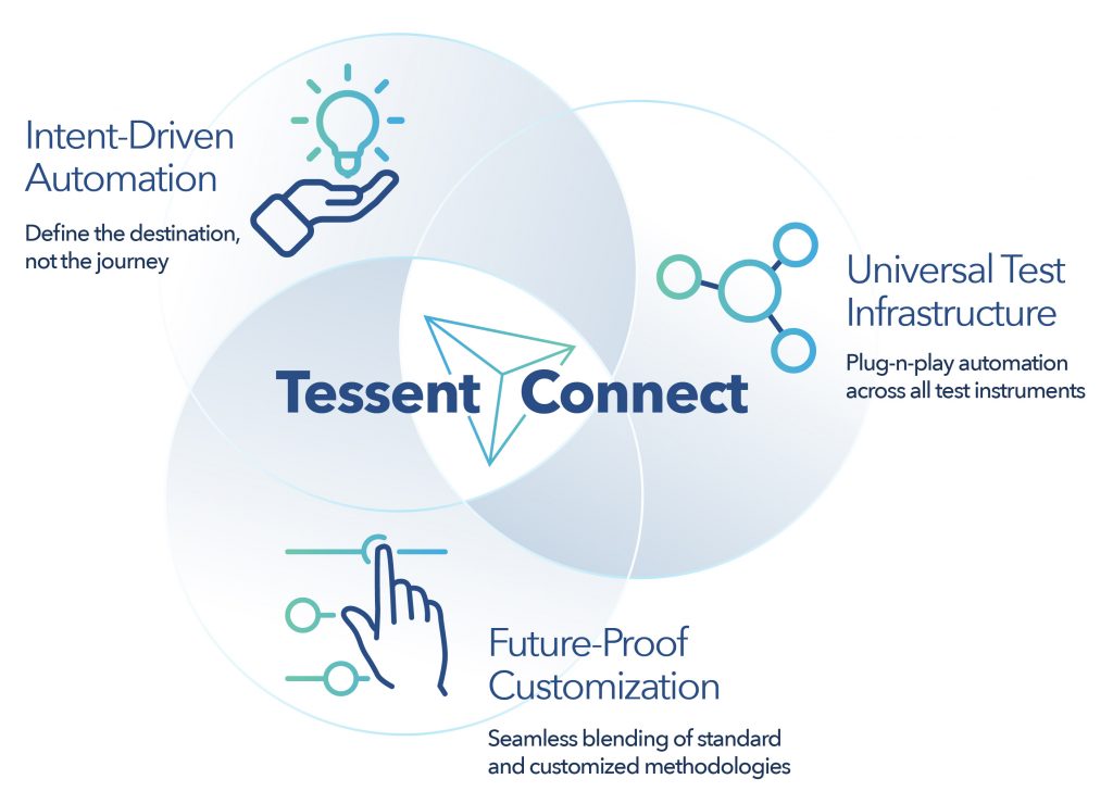
Another way of improving the DFT flow is to push more of the work up into the RTL phase. This requires a merger of DFT flows with the standard front-end design flow, and that the DFT tasks be both automated and repeatable. Creating a reliable DFT flow is easier if all the DFT technologies are built on a shared database. A unified DFT platform can operate as an ‘intent-driven’ environment, reducing the complexity of the DFT flow and accelerating time-to-market. Both eSilicon and Broadcom have presented results showing 50% reductions in implementation time with hierarchical DFT and a unified DFT platform. (Figure 2).

Figure 2. Tessent Connect provides the type of platform necessary with current levels of complexity and integration (Mentor)
A winning DFT strategy is not just dependent on DFT tools, but also on the ecosystem around them. Partnerships ensure scalable technologies that work in any design flow. For example, for cell-aware test, you can make your own cell-aware models, but Arm now provides cell-aware library models for both ATPG and diagnosis. There are existing reference design flows for Mentor DFT with Arm and Samsung. ATE suppliers Teradyne and Advantest support over-the-cloud tester access and 1149.10 high-speed IO scan test in partnership with Mentor.
Summary
To remain competitive, your DFT strategy should offer more efficiency, better test coverage, smoother integration with flows and function system requirements, faster and more accurate analysis of production test results, and greater flexibility and usability. Investing in a reliable, market-leading DFT platform will confer an enduring business advantage for products today and the new challenges of tomorrow.
Further reading
For more information, download this whitepaper: “How to maximize your competitiveness in the semiconductor industry using advanced DFT”.