A better way to debug P2P results
P2P (point-to-point) resistance is fundamental to IC reliability verification. Handle it more efficiently with detailed, automated path layout analysis.
Thinking as a consumer rather than an engineer, what does product reliability mean to you? If you are like most people, you expect a product to work properly right out-of-the-box, and every time you turn it on or use it. You also expect the product to last for a reasonable length of time before requiring repair or replacement. ICs are just like every other product in the marketplace. They need to perform according to specifications, and perform properly for the intended life of the chip. IC reliability verification is all about ensuring these two market criteria are satisfied before tapeout.
If you’re a circuit verification engineer, you are already well aware of how critical accurate point-to-point (P2P) resistance and critical density (CD) simulation are to IC reliability. The ability to simulate circuit operation and identify and fix potential reliability issues before going to fabrication is essential to market success. At the same time, you are also intimately acquainted with how time-consuming and resource-intensive the process of debugging and correcting errors can be. Would it not be nice to have a little more help in that process? This article explores some options. but first, two quick primers on P2P resistance and CD simulation.
P2P simulation
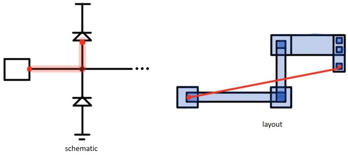
At the device interconnect level, P2P resistance simulations provide insight into how the parasitic resistance of net traces may affect circuit reliability, and whether the circuitry will perform as designed. A P2P resistance simulation measures the effective resistance of a current path by combining all the individual resistor bodies into a total resistance and determining whether or not that net exceeds a predefined resistance threshold for various device interconnect paths. Figure 1 demonstrates a simple P2P measurement from an input pad to an electrostatic discharge (ESD) protection circuit device — in this case, a diode clamp connected to power. For the circuit path shown in the schematic, there is a corresponding trace path in the physical layout.
When the combined resistance of the layout polygons that make up the net trace is higher than the allowed threshold, the trace path measurement is flagged as a P2P violation. To fix the resistance of the total path, engineers must identify which portions or segments of the entire path can be rerouted in a way that reduces the total resistance. Increasing the trace width and adding additional parallel paths or vias are two routing practices that can reduce the effective resistance of the overall current path.
For a simple net, engineers could just use manual inspection of the net layout combined with their experience to determine the correct fix. But when was the last time you encountered a simple net in your designs? In the real world, nets are usually very complex and identifying possible high resistance areas is a significant challenge. Engineers need more data to be able to quickly and accurately determine where a problem might lie and what fixes might be appropriate.
While a P2P simulation result provides engineers with a total effective resistance value for an interconnect path, this one value does not provide many clues about which smaller segment of the whole path should be investigated first when it is necessary to reduce the total resistance. Breaking the path into smaller segments, and then providing individual resistor body data (such as CD and resistance) for these smaller segments can help point designers in the right direction for layout adjustments.
CD simulation
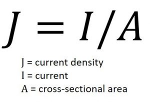
CD is the current divided by the cross-sectional area of a conductor. Figure 2 shows the elements of the CD calculation formula. CD simulations report the amount of current that will pass through each segment of the interconnect, enabling designers to locate specific points where the design could potentially fail due to excessive current.
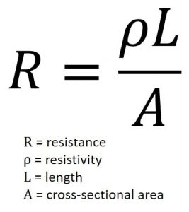
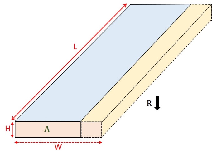
Resistance is the resistivity multiplied by the length of a conductor, divided by the cross-sectional area (Figure 3). The relationship of the CD of a path segment and its individual resistance can demonstrate how a high CD value can be a good indicator that the path segment is too narrow, causing a higher resistance contribution to the effective P2P path resistance.
While CD simulations provide valuable data in the physical verification process on their own, the CD values can direct engineers to those areas in the interconnect path that may be significantly contributing to the higher total resistance of the current path (Figure 4).
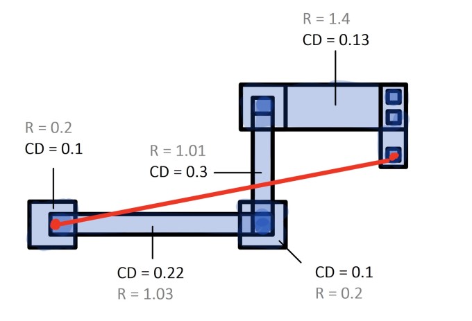
Figure 4. Identifying the CD value of each net layout polygon provides engineers a starting point for adjustments (Mentor)
You might assume that the individual resistance values for the path segment resistor bodies would suffice in determining where a higher resistance point might be, and this information is useful… to a certain extent. However, because CD values also factor in parallel resistances that reduce the effective resistance of the entire interconnect path, they provide more information than using just the resistance values of each individual resistor body.
For example, Figure 5 shows an interconnect layout in which an identical parallel path has been added to the total current path. The highlighted resistor bodies have the same individual resistance values regardless of whether there is a parallel path, but the total effective resistance is reduced by the addition of this path. The parallel path also divides the current that would otherwise have flowed only through the original path segments, reducing the CD values. What does this mean for you? The presence of relatively high CD values in a segment of an entire P2P resistance path is a strong indicator that the addition of parallel paths can reduce both the CD values and the total effective resistance for the P2P measurement.
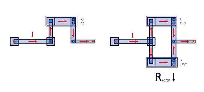
Figure 5. Adding a parallel path to an interconnect layout can reduce both the total effective resistance of the full P2P path and the CD values of the path segments (Mentor)
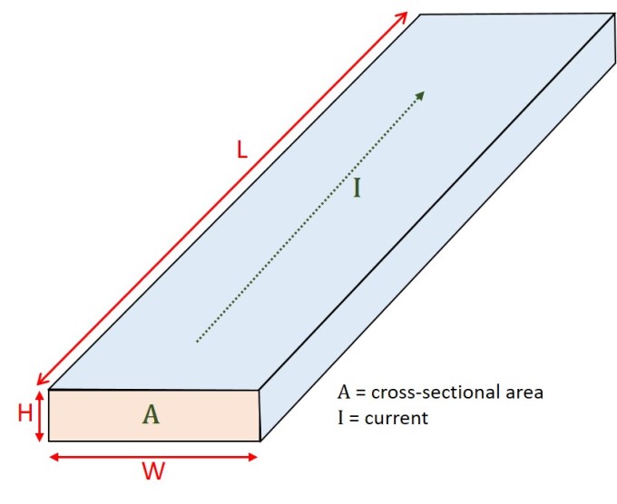
Given that both CD and resistance are inversely proportional to the cross-sectional area of a conductor, we can deduce that increasing the area decreases both the CD and the resistance through the conductor. In addition, if there is no change in conductor dimensions, we can also deduce that a higher CD value can be a strong indicator that there is a higher effective resistance contribution in the context of the interconnect trace polygons. Figure 6 shows what a cross-section view of a layout interconnect polygon might look like as a conductor whose resistance and CD are calculated using the given formulas.
In the case of an IC layout, the actual thickness of the trace (height portion of the conductor’s area) is constant throughout the design layer. Therefore, one way to reduce the CD of the polygon is to increase the trace width. This increases the conductor’s cross-sectional area, which is inversely proportional to the CD. Since the resistance is also reduced by the increased cross-sectional area, increasing the trace width lowers the polygon’s resistance as well (Figure 7).
Observing CD values for the path segments of a P2P resistance path is an effective way to determine which areas of the layout path are most likely to be causing a high total effective resistance. High CD values concentrated in a particular path segment can help engineers recognize where the addition of more parallel resistance paths, or an increase in trace width can reduce CD and reduce in turn the total effective path resistance to meet the P2P simulation thresholds.
Using P2P and CD data to debug resistance issues
While different EDA tools use different strategies, we will look at how you can implement a solution to resistance issues in your layouts using the Calibre toolsuite. By using the Calibre RVE results viewer in conjunction with the Calibre PERC reliability platform, engineers can view Calibre PERC P2P simulation results, and take advantage of several debugging capabilities to fix resistance violations.
A Calibre PERC P2P results database (RDB) reports any resistance simulation results that violate the thresholds specified in the Calibre PERC rule deck. However as stated earlier, one of the challenges engineers face during the P2P debug process is that they essentially have just one total effective resistance value for each effective resistance simulation in a P2P RDB. To identify and debug a potential problem area that may be causing the higher total resistance along the path of a P2P result, they need more information about the smaller path segments.
The Calibre PERC logic-driven-layout (LDL) P2P debug flow allows engineers to obtain more data about the smaller path segments for specific P2P results without re-running a full Calibre PERC simulation on an entire design. Because the Calibre PERC tool saves voltage propagation and cross-reference metadata generated in the original full-chip P2P run, engineers can ‘restart’ the P2P debug flow and save additional polygon data for specified P2P simulations in subsequent Calibre PERC runs. These subsequent P2P debug runs automatically produce an additional RDB containing parameters such as CD, resistance, and more for each individual resistor body (smaller path segments) in the path of the P2P results that were specified.
Using this additional data, engineers can then quickly determine how the individual segments of the interconnect path behave in the context of the entire current path. Using the Calibre RVE colormap and net layer highlighting capabilities, they can also get a visual display of where the higher resistance and CD values are coming from in the P2P result path. Here is a simple example.
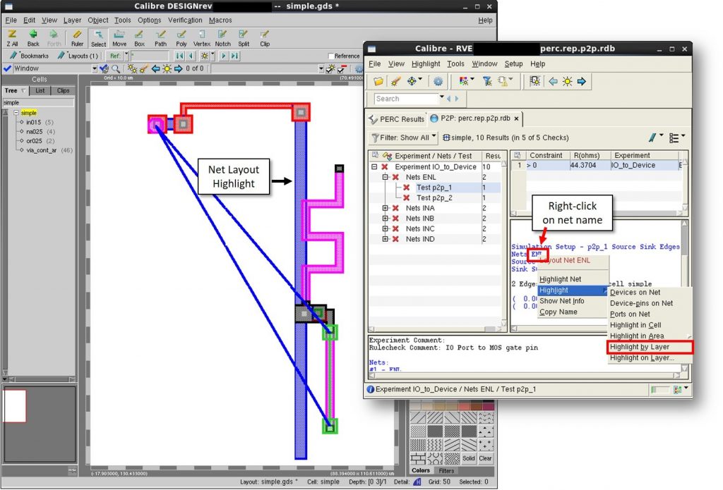
Figure 8 shows a layout design in the Calibre DESIGNrev layout viewer, with the Calibre PERC P2P results database open in the Calibre RVE results viewer. There are several P2P violations whose total effective resistance exceeds the resistance threshold (40 Ohms). Looking at the ‘Test p2p_1’ result, we see that the total effective resistance for ‘p2p_1’ is around 41.38 Ohms, slightly above the allowed threshold of 40 Ohms. Clicking on ‘Simulation Setup…’ in the Calibre RVE Details pane highlights the P2P simulation in the Calibre DESIGNrev layout viewer. The display includes the start and end points (sources and sinks) of the path included in the effective resistance value, as well as fly lines that connect and show the relationships of these points.
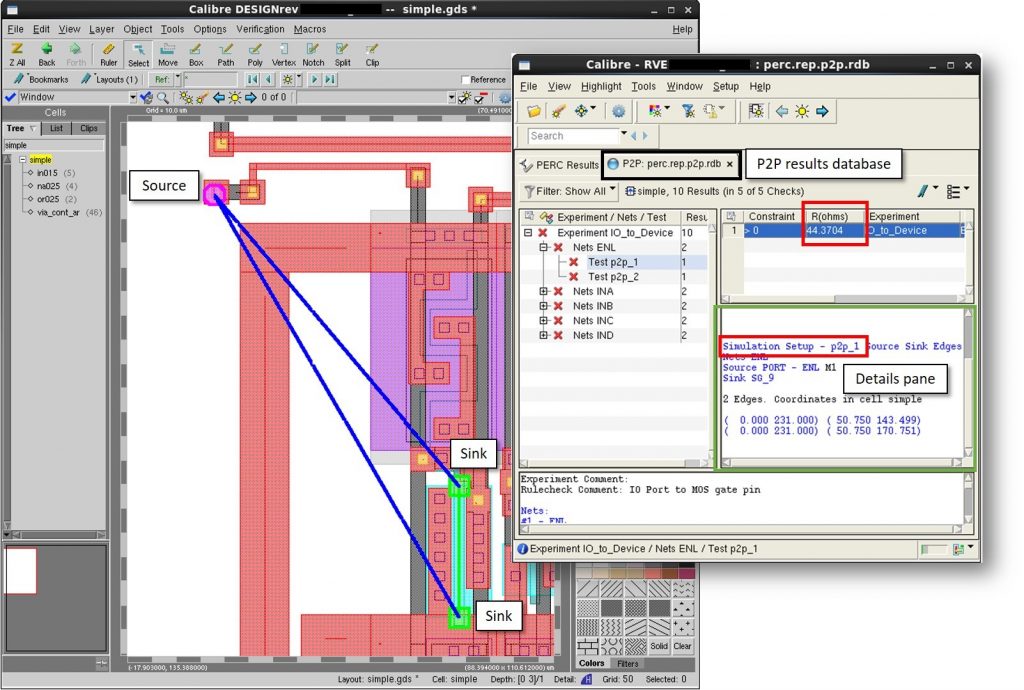
Figure 8. Calibre PERC P2P RDB opened in the Calibre RVE results viewer (Mentor – click image to enlarge)
To better understand what the current path looks like between the simulation points, we can highlight the layout net in the Calibre RVE results viewer to get a layer breakdown of a layout net in the Calibre DESIGNrev layout viewer (Figure 9).
Observing the P2P simulation sources and sinks in addition to the net layout allows us to quickly see which part of the design layout contains a violation, providing a great starting point in the attempt to reduce the total effective resistances of the result. However, to locate the segment of the path contributing the most to the total effective resistance, we still need more data about the smaller path segments.
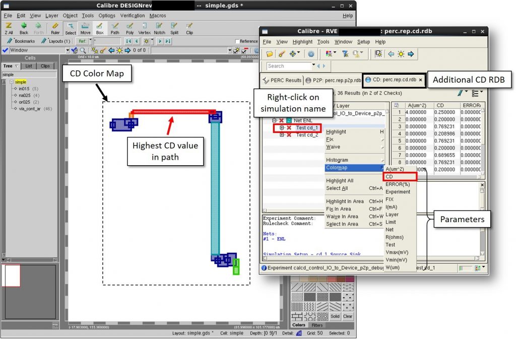
The next step is to run a P2P debug simulation on the P2P result of interest (‘Test p2p_1’). This flow produces an additional RDB containing parameters such as CD, resistance, and so on for each individual resistor body in the specified P2P result. With this RDB open in the Calibre RVE results viewer, we can highlight a colormap of the CD (or any of the other listed parameters) of each resistor body in the Calibre DESIGNrev layout viewer (Figure 10).
In the CD colormap generated using the Calibre RVE results, there is a segment in this particular path that has a significantly higher CD value than the other resistor bodies. Increasing the width of this section of interconnect should reduce the total effective resistance of the P2P result.
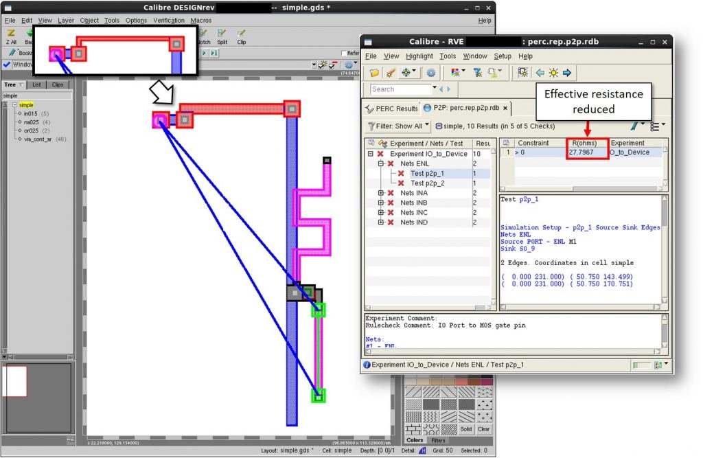
Rerunning the Calibre PERC P2P simulation after this change is applied confirms a significant drop in total effective resistance (Figure 11). Simulation ‘p2p_1’ is now around 27.80 Ohms, down from 41.38 Ohms.
Summary
P2P resistance and CD simulations are critical elements in the IC reliability verification process flow. However, debugging and correcting errors can be time-consuming and resource-intensive. Using additional debugging data helps engineers quickly find the likely problem areas in the interconnect. With a detailed analysis of the path layout, engineers can more quickly and accurately identify, correct, and verify P2P violations in their IC layouts. Enhanced verification strategies such as these help ensure reliable performance and consistent product lifetimes, enabling companies to market and support their products with confidence.
Related Links:
White paper: Debug P2P results using resistance and current density data
How-To video: How to debug P2P results
About the author
Slava Zhuchenya is a technical marketing engineer supporting Calibre interface tools in the Design-to-Silicon division of Mentor, a Siemens business. His primary focus is the support and enhancement of the Calibre RVE and Calibre Interactive products. Previously, Slava was a member of the Calibre PERC R&D team. He received a B.S. in electrical engineering from Portland State University. Slava may be reached at slavaUNDERSCOREzhuchenyaATmentor.com.
