Facing the verification management challenge
The growing verification challenge, and how to address it by coordinating multiple debug strategies.
The integration of multicore CPUs, graphics coprocessors, modems, multimedia and networking facilities in the SoCs that power today’s sophisticated smartphones, tablets, computing and networking devices is creating a new verification challenge. The divide-and-conquer approach that worked well when such systems were built of interconnected chips is less effective now that their functions are integrated on one die, with complex specifications, rapidly increasing software content and relentless pressure to get the design to market.
Today’s verification challenge is immense. One SoC may be defined by more than 30 million lines of design RTL and testbench code. It may embed 10 or more sophisticated communications protocols (think USB, and mobile connectivity on a handset, for example), and have as many as 200 power domains to optimize energy consumption. Verifying such a chip may involve using thousands of servers, many with 150Gbytes or more of memory, writing and testing hundreds of thousands of assertions, and producing and interpreting terabytes of coverage data.
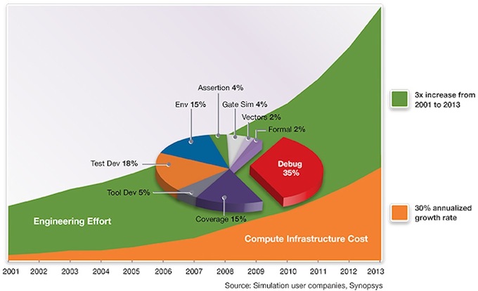
It’s little wonder, then, that the cost of verifying a leading-edge chip has risen 30% a year since 2001, so that it is now three times what it was back then, and that verification engineers outnumber design engineers by two to one.
Figure 1 The growing cost of verification (Source: Synopsys)
To tackle the verification challenge, design and verification managers must find ways to achieve a series of order-of-magnitude productivity improvements in their verification strategies. This may mean greater reuse of testbenches, updated methodologies, and the authoring and application of verification IP. They will also have to leverage next-generation technologies that enable significantly more throughput from their server farms, and introduce debug automation and debug strategies that can detect and prevent more bugs, more quickly.
Time to market is key
The relentless competition in consumer and other markets is creating tremendous pressure to tape out designs. This pressure is intensified by the increasing complexity of the core SoCs, which integrate ever more digital functions, are adding analog functions, implement sophisticated power-management strategies, and embed a rapidly growing amount of software. For design and verification teams, this means that the challenge is evolving from taping out a functional hardware design to delivering that hardware with correctly functioning software onboard as well. This added complexity now increasingly drives decisions about verification strategies.
Performance matters
Due to the complexity of today’s SoCs, leading-edge chip design teams must apply a variety of verification techniques to gain the confidence to tape out a design.
Exhaustive simulation demands large server farms, and some companies are spending millions, if not billions, of dollars to build and run the IT infrastructure necessary to do high-performance verification. The total cost of ownership for these server farms includes the cost of acquiring the hardware and regularly updating it, powering and cooling it, and administering the whole set-up. No company wants to incur these costs, but they know that every improvement they make in verification performance will have a material effect on their bottom line. They also know that the cost of missing a market opportunity because of a faulty chip is so punitive that teams must run as many simulation cycles, and get as close to full chip coverage, as they can.
To achieve improved verification performance, companies are turning to techniques such as constrained random verification. This involves writing complex testbenches that generate random, but meaningful, vectors for the design. These testbenches themselves must be verified before use, a process that can be accelerated using fast constraint solvers. The better the testbench, the more effective the test, and hence the greater the return on the IT infrastructure that runs it. So performance, whether it is measured in pure CPU cycles or the effectiveness of a particular testbench, is critical to meeting the ‘time to tape-out’ and ‘time to software’ challenges.
Debug challenges multiply
Surveys and studies suggest that 70 percent of the effort involved in taping out a complex SoC is spent on verification. Half of that, or 35 per cent of the total, is spent on debugging the chip, the interaction between the chip and its software, and the testbenches.
The scope of debug is also growing, as issues such as power management, hardware/software co-design, and the introduction of analog or mixed-signal blocks, create new challenges.
For example, turning a chip’s functional blocks on and off to reduce power consumption introduces thousands of unknown (X) states during simulation, which then have to be sorted into real bugs and simulation artifacts and correlated with the designer’s power intent. X-propagation has always been difficult to debug, but with low-power designs, both the verification and debug processes require the X states to be modeled more accurately and to be propagated more correctly during simulation.
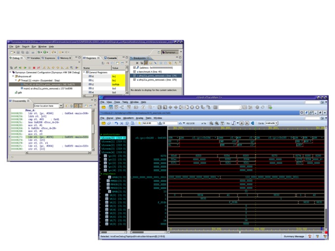
In hardware/software debug, designers need to be able to see the relationship between their C or assembler code and the RTL with which it was interacting when a fault occurred. Debugging the interaction of analog or mixed-signal blocks and digital blocks introduces another set of challenges.
These are just some examples of the way in which the scope of the debug task is broadening. What makes the issue even more challenging is that these debug domains interact – a faulty analog circuit may create a digital logic bug that causes the chip’s software to misbehave.
Multiple strategies
In the face of these challenges, design and verification managers must develop a set of strategies that, working together, provide them with a level of design coverage and debug insight that gives them the confidence to tape out the chip.
This means making trade-offs between various forms of verification, in terms of their coverage, speed and costs, and various forms of debug, in terms of their efficacy. It also means taking into account the costs of moving from one approach to the next and the possibility of introducing inconsistencies as they progress from approach to approach.
There is no standard verification strategy. For example, in one market sector I have seen two companies making competing chips that use verification strategies that are almost polar opposites. One company builds FPGA-based prototype boards in order to run as many cycles as possible. The other relies on simulation and coverage management and rejects hardware prototyping. The right approach is to use both. Essentially, one should use all possible strategies at one’s disposal. There is no one-size-fits-all approach.
The challenge for design and verification managers, and the tools vendors that support them, is to raise confidence in each methodology, and to make it possible to move between approaches very easily. For example, standard server-based simulation offers flexibility, so long as compile times remain within practical limits. Emulation offers greater speed, once the design has been set up on the emulator. An FPGA prototype might be even faster, but it will lack the access to internal signals of a simulator or emulator.
The difficulty for managers is to understand the tradeoffs involved in each of these approaches and how to move between them for the best overall result. For example, different design teams will hand off from simulation to emulation at different points in their process, depending on how confident they are with the revisions they are likely to need to make. In a simulation, the typical change-and-compile cycle is 3 to 4 minutes. In emulation, making the same change takes a bit longer so verification teams need to reach a version of their design that is a bit more stable before moving to emulation.
Design managers also need to marshal the skills that support each strategy, from server-farm management for the simulation phase to design-partitioning and logical-to-physical mapping in the FPGA prototyping phase. The skill here is to know when to make the transition between each verification approach for best overall effect, and then to have the people and resources on hand to make that transition as smooth as possible.
Debug roadmap
The broadening frontier of the debug task makes the verification issue more complex. Along with knowing when to move between different verification strategies, and how much verification is enough, design managers also need to develop a consistent debug strategy for the various forms of verification. Currently, there is no systematic unified debugger that works across all these different ways of exercising a design.
As a step towards a more systemic approach to debug, Synopsys has acquired SpringSoft so that we can offer the de facto standard Verdi as an open platform upon which users, third parties and ourselves, can innovate effectively by offering plug-ins and extensions to tackle emerging debug issues.
Figure 2 Verdi's hardware/software debug facility synchronizes RTL and programmer views (Source: Synopsys)
Verdi has powerful underlying abilities, such as an understanding of how a design is synthesised from RTL into gates that is expressed in a single database, which others will be able to build upon. We’re already adding ways to show verification coverage in Verdi’s graphical user interface, so that users can relate coverage and debug. We will soon be adding new capabilities, such as hardware/software debug and support for analog and mixed signal debug, over time.
Verification management
Design and verification managers will need technologies with which they can see how the many forms of verification and debug interrelate, so that they can develop better insights into the tradeoffs they are making as a design progresses to completion. Such technologies should be flexible enough to handle many forms of verification. They should also be able to present many types of metrics, and do a good job of turning those metrics into actionable information upon which design managers can make timely decisions that lead to the most efficient and effective overall verification strategy for their designs. And they should enable design and verification managers to explore a variety of verification strategies against key parameters, such as coverage and cost.
There’s one truth that the managers of large SoC projects must live by: time to market is king. Effective verification strategies, be they better ways to write testbenches, greater reuse, or a well thought-out approach to debug, are vital to getting big designs out of the door on time and with a reasonable level of confidence.
Michael Sanie is senior director, verification marketing, Synopsys

