Manufacturability and yield toward 22nm
This year’s Design Automation and Test in Europe conference heard from a broad range of users and suppliers about the challenges to and solutions for getting optimal yields at advanced process nodes, particularly as the industry advances toward 22nm. This article recaps presentations by four executives at the Dresden-hosted event: Pierre Garnier of Texas Instruments, Joe Sawicki of Mentor Graphics, C.J. Clark of Intellitech, and Naveed Sherwani of Open-Silicon. The presentations were all given during a session entitled “The Impact of Nanometer Technologies on Manufacturability and Yield.”
As we move toward smaller manufacturing process nodes, chips continue to encounter more manufacturing defects, be they parametric, systematic or random.
Yield has always been a fundamental part of semiconductor design. If you can’t make it, you can’t sell it. However, a new wave of innovation in design-for-yield is underway to address the physical challenges of sub-micron design, the pressures exerted by increasingly complex integration as well as shrinking design and product life cycles, and the profitability lost within even a poorly yielding yet sellable SoC.
Even apparently small improvements in yield can have a significant impact on the bottom line. Research undertaken by IBM at 90nm famously found that on a run involving 30,000 wafers a month, a 1% improvement in yield could increase the output of chips by 1.4 million units a month.
Another way of looking at this is offered by Texas Instruments. If you can save 10¢ a unit on a chip that is selling one billion units a year, that represents $100m straight back into your coffers either as profit or for investing back in further designs to broaden the product range. Even when you can sell it and make it, you may not be making anywhere near as much as you should.
This article extracts highlights from four presentations at this year’s Design Automation and Test in Europe (DATE) conference, held in Dresden, Germany (March 8-12). The speakers were:
- Pierre Garnier, vice president and general manager, Texas Instruments (TI);
- Naveed Sherwani, president and CEO, Open-Silicon;
- Joe Sawicki, vice president and general manager, Mentor Graphics; and
- C.J. Clark, president and CEO, Intellitech.
Each talk is discussed in this order and the article will then conclude with some general observations that link the quartet. It is nevertheless worthwhile stating from the outset that an over-arching theme for the session was that there is no universal panacea for yield. Rather, such manufacturability issues require ubiquitous consideration throughout a design flow, and involve securing access to a heavily laden toolbox.
The chip vendor
Pierre Garnier offered a ‘management level’ perspective on the challenges in SoC design. In his role leading TI’s baseband efforts in Europe, he described the wireless sector as offering a particularly good example of the main pressures facing chip vendors today and a space in which they were being addressed and overcome. “It is a market that is stretching our engineering capabilities and our manufacturing capabilities to the greatest extent,” he said.
Garnier characterized these challenges from a number of perspectives. From a technology point of view, he noted that after a great debate about ‘convergence’ and whether it was going to happen based around, say, the TV or the PC, it was now in fact progressing most rapidly in the mobile device space.
“We are today shipping applications processors of more than 1GHz that can do full HD, let you browse the Web at the same speed you used to on your home computer, and that allow you to recharge the end-device only every three days,” he said. “That is today’s challenge—bringing not only that capability, but doing it at low power. That is what is driving us.
“The next challenge—and we are already busy with it—is how to drive a user experience that goes outside the physical limitations of a device that must still fit in your pocket. So, you are going to be leveraging things like 3D imaging and resolution as well as new camera technologies. You will do all this with a single SoC that manages all the protocols and all the software and all the processing required.”
Added to that are the pressures applied by demand and time-to-market. “We are shipping more than 1.2 billion cell phones on the planet every year and this trend is not slowing down,” said Garnier. “Also, the OEMs always want us to do more, faster and better, and at lower cost.”
Then finally, he noted that wireless SoCs are now one of the growing number of design categories where a project needs more software than hardware engineers.
The TI approach
Garnier explained that concurrency has become central to the way in which his company now attacks new designs.
“The semiconductor guy in the mobile industry does not provide a chip,” he said. “We provide a platform with full software embedded on it, integrating a high-level operating system—be it Symbian, Android or MeeGo or whatever. It has to have full capabilities to run the applications, the drivers and the user experience. It has to have undergone all the relevant integration. So, before the first internal sample of the silicon gets to the lab, you have to have all the software already developed.”
This involves complex hardware emulation, and also an ability to review a complicated set of trade-offs at the architectural level, especially when your concerns are not only megahertz but also milliamps. Achieving such integration—effective hardware/software co-design—has already begun to pay off for TI internally, according to Garnier.
“When we got our latest generation of application processor for the mobile industry in our labs, 10 days after we received the first sample, we were able to run 80% of the full capabilities with both Symbian and Android. In just 10 days—because everything had been developed in a concurrent manner,” he said. “More important, after two weeks, we were able to launch the device to key customers and demonstrate its capabilities.”
This kind of target schedule is expected to become increasingly common throughout the silicon industry as device lifetimes threaten to become shorter than design cycles. Once you could maybe miss a few months for a respin and still extract some profit—today, such delays are, as Garnier noted, “deadly.”
In this context, Garnier’s main message for the DATE audience was less one concentrated on the concurrency gospel that TI aims to spread internally, and more about how that also has to impact on its relationships with other players in the development process, especially when it comes to manufacturability and yield.
“It also stretches to manufacturability, to design for test. We leverage a lot of partner capabilities, at the foundry level and also for assembly & test. This is very important,” he said. “You need cross-functional teams from product engineering to process development to assembly & test. In fact, that last one is growing because we now have 3D packaging and we are shipping tens of millions of those packages every month. The yield on those products counts for a lot.” Garnier added that this level of integration has presented “managerial and organizational challenges,” but these were inevitable.
“We are working on the steepest ramps we have ever seen. We have moved into a new product, qualified it and got output to 50 million units inside three months,” he said. “You cannot go for that with a yield that is not optimized.”
The custom design vendor
Naveed Sherwani focused his presentation on one contention central to a less obvious aspect of the yield issue: “Power estimation and power design are still not parts of a well understood science.”
He started from the position that because of emerging power variability, a chip can appear to yield because it is functional, and therefore might pass test. But it could exceed or fail to reach its power budget.
“It is a very tricky situation,” Sherwani said. “From the fab’s perspective, the chip is completely functional in the sense that there are no defective transistors and they are working as predicted in all the models. But the power is not where it needs to be.”
He saw part of the problem residing in the fact that a design team typically cannot define how many transistors on the chip will be turned on and off. It is a question that no model as yet can answer. So, what designers need to do is look at applying a very broad range of techniques that can be used both pre- and post-fab.
“When dealing with power, I think everybody knows that the focus has to be on leakage,” said Sherwani. “Most people will address this with some kind of clock gating. They will do some kind of power gating. And there can be low power placement, multiple threshold voltages, and multi Vdd is now common. And it doesn’t end there. You can do voltage scaling, multi-channel scaling, multi-channel lengths and so on. The toolbox has in it a lot of common techniques.”
However, as that last comment suggests, Sherwani wanted to discuss three less common techniques that Open-Silicon now uses in developing SoCs and ASICs for its clients. These are transistor-level transformations, power recovery and back biasing. They fit within his company’s overall design strategy under the PowerMAX banner (Figure 3).
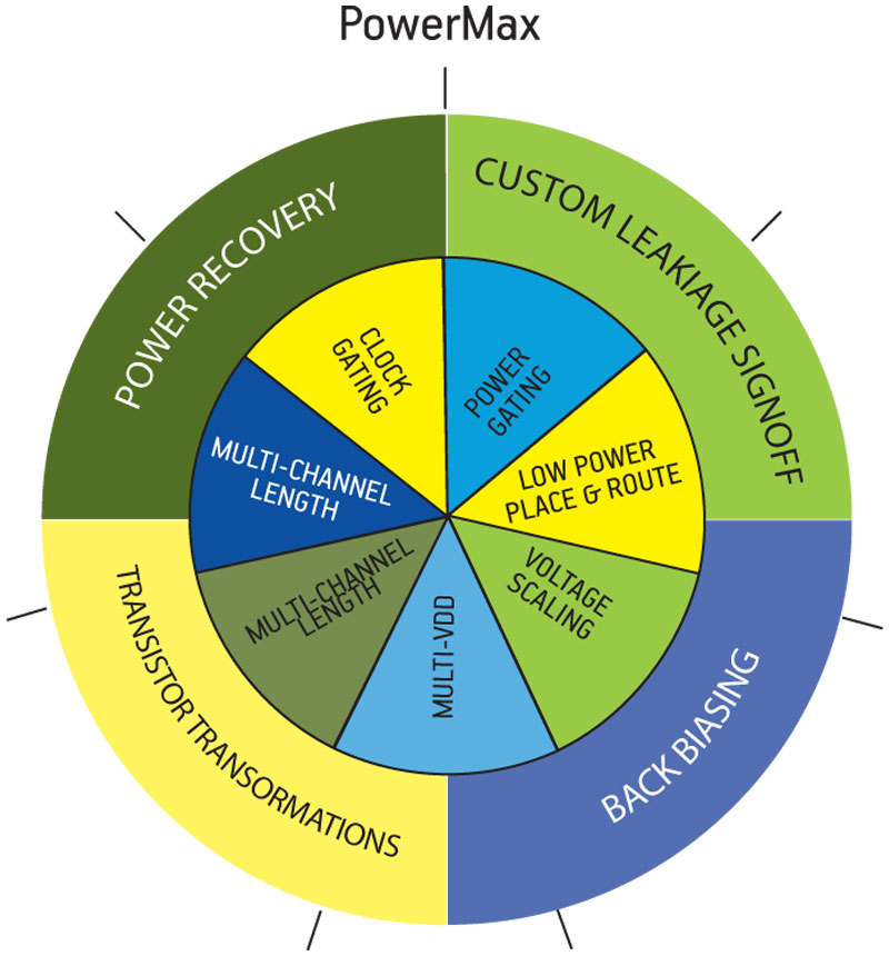
Figure 3
The PowerMAX toolbox
Transistor-level transformations
“Transistor-level transformation is conceptually a very simple technique but also one that is very hard to accomplish,” said Sherwani. Indeed, the expertise that his company acquired and has subsequently developed in this area with its purchase of Zenasis Technology extends to seven-and-a-half years of research and two million lines of code.
“What it involves is that after synthesis, we study the different clumps of cells on the chip and see if there are ways that we can combine some of them,” Sherwani explained. “Let’s say that we have put certain cells in our library. We might see that there are 100 cells that we can add specific to that design and eliminate cells from the library. We create the cells on the fly by register-specific algorithms and then characterize and reinject them into the cell library.” The result, Sherwani said, can reduce both dynamic and leakage power.
Power recovery
Sherwani’s contention here is that by again analyzing a design after synthesis, you can detect a number of paths that are over-optimized because they are not on the critical path, so you can relax the threshold voltages along those non-critical connections.
“It is actually a very straightforward technique,” he said. “And what it shows you is the toolbox nature of the problem. You might only get 3% or 4% improvement on this, but if you have that toolbox and you use all 15 or 16 things in it—the power recovery along with the gating and placement and the transformation—then suddenly you start getting improvements of 16% or 24%. Yes, those are remarkable numbers, and you don’t get them very often, but this is largely about taking a very broad strategy.”
Back biasing
Unlike the two other techniques that Sherwani discussed, back biasing is applied to the design but largely for use post-fab. “On a typical process corner, you can lose about 7% of your chips because they do not meet the power budget; the parts will not be useful for the end application,” he said. “You can do a few things with the design margins, the CD [critical dimension] margins, the power margins—but, at 40nm, things are already getting ridiculous. There’s not much you can do here.
“We have tried to do something different. We are designing some structures on the silicon and then we later try to use them to recover power—it is post-silicon tuning of the chips in that sense.”
These structures allow you to move the voltage for a chip in such a way that you can change the power curve of each transistor. In some cases—Open-Silicon has used the technique on around 25 designs so far—the design has been able to move power by as much as 42%, though results in the 12-14% range are more common.
“From a yield perspective, these are very big numbers—you can save a lot of silicon,” Sherwani said. “On a broad level, the highest leakage reduction we have seen at 65nm is about 45%, and for 40nm we think we can get that to 80%. That translates into a yield improvement of about 5%.”
The one caveat that Sherwani added for back biasing as opposed to the two other techniques was cost. “We think that it is something for high-volume silicon,” he said. “The combined design and IP costs for back biasing on a 65nm chip are going to be in the region of $600,000-$700,000. So you obviously need to be running a lot of devices to grab that back. Otherwise, you might as well take the hit.”
The EDA vendor
Joe Sawicki expanded on Garnier’s point about how extensively design-for-manufacturing (DFM) techniques need to be deployed and also described how big a toolbox the job needs within a concept he described as ‘Pervasive DFM’. “DFM really needs to touch on all the major phases as a design starts as a concept and goes through implementation, down through test and assembly,” he said.
He described how this philosophy has already been extended into various stages of the design flow, including place and route (P&R), modeling for verification analysis, mask resolution enhancement, test and—increasingly—advanced yield learning. For each category, Sawicki cited examples of recent developments (Figure 4).
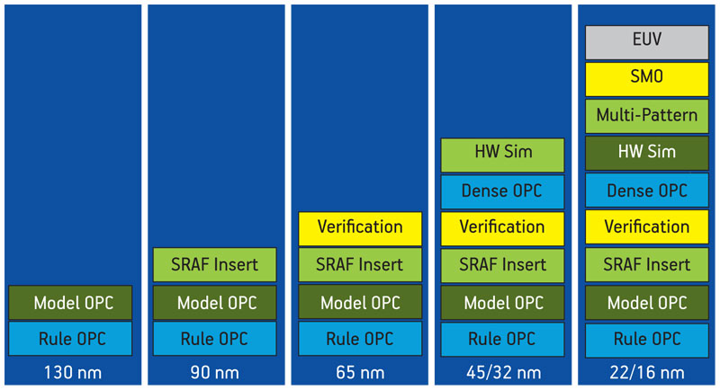
Figure 4
The increasing importance of DFM in manufacturing
Today’s toolbox
Routers traditionally have emphasized spacing and width but already there is work toward bringing in more complex items such as the latitude for jogging or for wide metal-to-short metal spacing. Issues that used to be a problem at the fab are being brought back up the flow to fix the chip before it moves to any kind of formal manufacturing steps.
“Classically, the approach has been to run the router from the P&R environment with its internal DRC [design rule check] engine and then run what comes out of that through a separate DRC signoff tool. What you’re seeing now is a trend for signoff tools to be bound into the P&R environment. This allows us to take the chip assembly step that can take a week or two after tapeout and instead close it off in a day,” Sawicki explained.
He added that lithography analysis is also becoming an important part of P&R where known defects are effectively self-repaired before the design moves on. Models, meanwhile, are also being used to check and optimize increasingly sensitive design tasks such as chemical-mechanical polishing (CMP).
“CMP is becoming a very important issue here and not just because of the planarity and its relationship to the variability of resistance and capacitance, but also because it has been found to fairly drastically affect things like stress,” said Sawicki. “In this case, technology’s been built that allows us to do a simulation of what the yield and/or planarity effect of the fill will be. You can tie that back into the design so that you end up with the least possible fill to achieve the best planarity.”
Mask resolution enhancement has undergone a number of innovations since optical proximity correction (OPC) first appeared at the 180nm and 130nm nodes. Sawicki described how, for example, 90nm brought sub-resolution assist features, items placed next to regular lines on the mask but which did not print on the wafer. They functioned to reduce variability, increase CD uniformity and enable much smaller features. Then, 65nm saw more sophisticated verification, while 45nm and 32nm ushered in a new generation of OPC techniques as well as more hardware simulation.
“Then at 22nm and 16nm, because we’re coming to the limits of how much resolution you can pull out of a system, we’re seeing things like source mask optimization, double- and multi-patterning and double dipole lithography as well as potentially EUV [extreme ultraviolet lithography],” said Sawicki.
We are now at a point where such fine adjustments must be made to the edges of lines and the work needed to compensate for sub-wavelength lithography is so complex that the pattern on the mask may look nothing like the design intent. Indeed, a comparison of the computing power required to undertake today’s enhancements really underlines how subtle things are getting.
“To produce the mask at 65nm, you’re looking at about 150 gigaflops of computational load, and we’re able to do that on about 200 CPUs running for 12 hours,” said Sawicki. “At 22nm, you’re looking at the need for about 20 teraflops. To put that into context, the world’s largest supercomputer was not capable of that level of performance until 2001. However, today, we can take advantage of distributed processing systems tied together with gigahertz Ethernet and do that with a standard cluster—you’re looking at something in the region of 1,000 cores.”
Tomorrow’s yield learning
With all the techniques mentioned above already in play (with others besides), there is now another level of sophisticated analysis being introduced to, again, attack the yield issue. Traditionally, identifying systematic defects has been a laborious process. You bring in failed chips, scrutinize them very closely, check them off against patterns on the wafer, perform structure analysis and root-cause identification, and finally try to tie all of this activity back to a correct batch. It can take a month or so, and that is when you are working with one of the better labs.
“So what we’re looking at is a change that really leverages normal production chips to allow yield learning,” Sawicki said. This will be based on methodological elements such as volume diagnostics and hardened test programs that are mined using statistical analysis so that you start to identify which areas are most fertile for yield learning.
Sawicki said that this had already begun to return dividends. “In one case, it led to the detection of an ever-so-slightly misaligned pellicle within a scanner that was causing a slight difference in the depth of focus that was then exacerbated by a CMP pattern across the wafer,” he explained. “By just taking the diagnostics from the test failure vectors coming off the scanner and running through statistical analysis, they were able to drive the problem back out of the fab and fix the alignment in the CMP process. And it didn’t just save a lot of failures—it helped identify areas of the chip that suffered from lower reliability.”
The test vendor
Test escapes are a serious problem. In 2007, IBM reported that they had a 99% fault coverage rate for stuck-at faults but only an 85% rate for transition or at-speed fault types. At the same time, Cisco Systems also released data showing that 68% of its system-level failures on equipment were attributable to the ASICs inside them. In his presentation, C.J. Clark concentrated on the degree to which these numbers could be attributed to the gap between the ‘ideal’ and ‘reality’.
“What’s the problem here?” he wondered. “It is that the tester has a perfect environment, but in the real-world system, the IC is subjected to a much different environment—there are temperature changes, there are tin-can oscillators, and all that.
“Also on the tester we have full pin access, so we can run BIST [built-in self test] and full vectors with that. In a system, you can’t. The pins are in their normal mission mode.” He described the key to all this as, in an echo of the famous real estate slogan: “correlation, correlation, correlation.”
“We need to be able to correlate the data that we see in the system environment with what we see back on the testers. Or we want to take this data and plug it into the simulator environment. Or we want tools that will allow us to identify the failing flip-flops. All this is part of reducing the test escapes and therefore improving the yield.”
Meanwhile, as in every other part of the design flow, there are heavy time-to-market pressures on test. A traditional ramp from first silicon up to full production can last 24 weeks, but vendors want to get this down to four to eight weeks if possible.
Today’s and tomorrow’s tools
Clark said that there are already a number of tools at engineers’ disposal to achieve these kinds of improved visibility in a timely way. One of these exploits the IEEE1149.1 standard on test access ports (TAPs) and boundary scan.
“People have long focused on the boundary scan path, but you can do a lot more. You can use 1149.1 as a way to get access to on-chip infrastructure IP in a system environment. You can have accessible monitors for voltage and temperature through the standard, accessible silicon debug units, clock control units and more,” said Clark.
Meanwhile, JTAG, used with tool command language (TCL), also provides important access to an in-system IC. However, there is now something else on the horizon. “The IEEE is working through another standard, P1687, which is currently a draft for the access control of instrumentation embedded within a semiconductor device—‘instruments’ being the preferred term in that context that covers infrastructure IP like BIST,” said Clark.
The standard provides a common language, offers a refined way of collecting data in the field, addresses multicore systems and establishes the kind of access needed to work with 3D stacks. Its context and implementation flow are shown in Figure 5 (p. 28) and Figure 6, respectively.
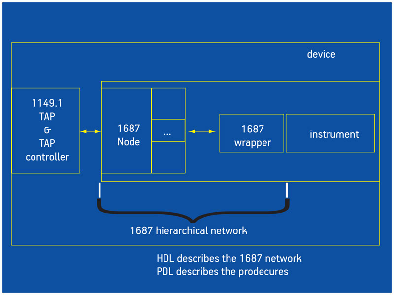
Figure 5
P1687 context
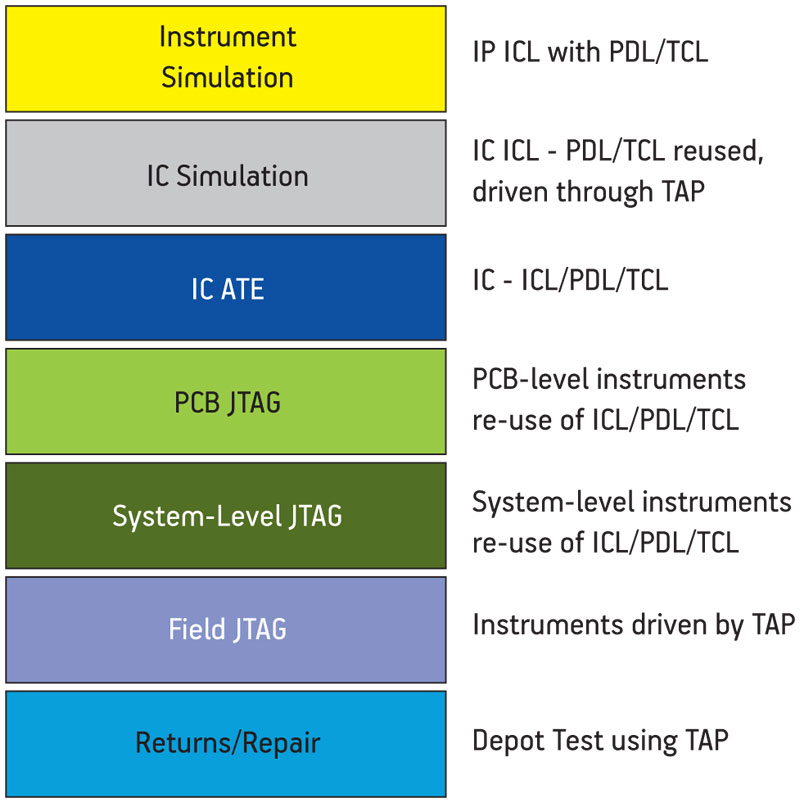
Figure 6
P1687 instrument verification/test flow
“It’s probably the only method that will give us access to these instruments in 3D,” Clark stresses. “It will make life a little easier with common languages that we can use at different phases of the IC life cycle.”
Conclusions
Yield enhancement has always been critical to profitability, but as product shelf-life shrinks alongside design cycles, there is less and less time to ascend the most efficient production ramp. Established DFM technologies can be brought to bear on this problem throughout the design flow rather than simply in terms of first silicon analysis. However, there are many options in an engineer’s toolbox and careful choices must be made as to which are appropriate for any project—some combinations may only be justified where volumes will definitely be very high, some may apply because performance is a priority and others because power is a priority (and still others will apply when both those masters will be satisfied).
However, for any design below 90nm it can now safely be said that there will be no such thing as a single DFM tool—there will always need to be several visits to one’s arsenal.
There was one other good takeaway from the DATE session. All four speakers were extremely optimistic about the industry’s ability to actually solve the problems now emerging on the path to 22nm.
In some cases, new techniques and standards promise to help—however, as much as anything, it is the intrinsic ability of engineering to maintain its own exponential in innovation that the panel believed would drive semiconductors and systems forward.
Design Automation and Test in Europe was held 8-12 March, 2010 in Dresden, Germany. Information on proceedings and future conferences in the series is available at www.date-conference.com.
Texas Instruments
www.ti.com
Open-Silicon
www.open-silicon.com
Mentor Graphics
www.mentor.com
Intellitech
www.intellitech.com