DFM matures
Engineering managers need to get their priorities in order for incoming process nodes, says analyst Gary Smith
You may have noticed that there are not too many design for manufacturing (DFM) panels taking place today. Most of the controversy seems to have been taken care of and it is common knowledge that the new semiconductor nodes will use both DFM and restricted design rules (RDRs). There is not even much doubt as to who the leaders are in the field with Synopsys and Mentor Graphics comfortably in first and second positions, switching places periodically (Figure 1).
After a dip in 2008, the forecast now points to an impressive 19.1% five-year compound annual growth rate (CAGR) for DFM tools. That is far above the overall CAGR for EDA. DFM is growing to be one of the major sub-applications, and it is therefore key to sales volumes for the major players (Figure 2).
DFM at 45nm
At 45nm, we are seeing all the fabs insist on the imposition of at least three RDRs. These rules are nothing dramatic and really should not get in the way of design engineers’ progress, although they still are not happy about it. However, one term now being thrown around is ‘slippery fish’, because the number of rules keeps changing at each process node. Some say we are looking at 100 or more rules at 32nm and 250 or more at 22nm.
Most engineers expect no major changes over an EDA tool’s lifetime, which typically covers two process nodes. Actually the fabs would also be very happy to just introduce new RDR requirements every two nodes. It would help their yield. Unfortunately for them, the demands from their customers are making that competitively impossible. Engineers want the fewest restrictions possible, so the fabs are forced to add the new rules at each node.
So what is everyone complaining about?
If you look at how the rules are being implemented, it appears that the design engineers are overreacting. Most rules are implemented in the physical libraries. Complaints about less performance are most likely attributable to the fact that the actual transistors are not speeding up as fast as we have seen them do in the past. Let’s face it—CMOS as a process is running out of steam. We are doing our best to push it along the Moore’s Law curve, but it looks like it has less than 10 years to go before we have to move to another semiconductor (or non-semiconductor) design fabric.
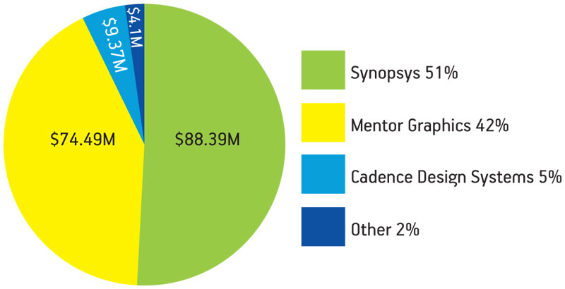
Figure 1
DFM market share 2008.
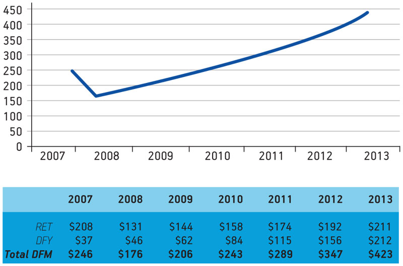
Figure 2
DFM forecast 2009 in $M.
The other complaint is that RDRs will make the die size larger. This could be true in some cases, but with pure logic, our willingness to allow engineers to put their transistors wherever they please has greatly lowered routing efficiency—often a fully routed system-on-chip (SoC) die is only 65% utilized. Indeed more frequently, RDR-routed die are more efficient than the freewheeling layouts of the past.
But what about the second tier guys?
There is a lot of concern that ‘upper mainstream’ designers, those in the second tier, will not be able to handle the increased complexity inherent in the increasing number of RDRs. That should be a concern—however, those engineers have a lot more to worry about than just those rules.
A few years ago, there were plaintive cries that the cost of designing SoCs was becoming prohibitive. But there are still plenty of new SoC products reaching the market and not just from the IDMs. We took a look at what was going on and found that the problem was real, but only among the upper mainstream users. What was happening was that the cost of design of an upper mainstream design flow was becoming uncompetitive compared against the cost of design based on a ‘power user’s’ flow.
A funny thing happened at the turn of the century. For the first time, the power users spent more on EDA tools than the upper mainstream, and that second tier share has been headed downhill ever since (Figure 3).
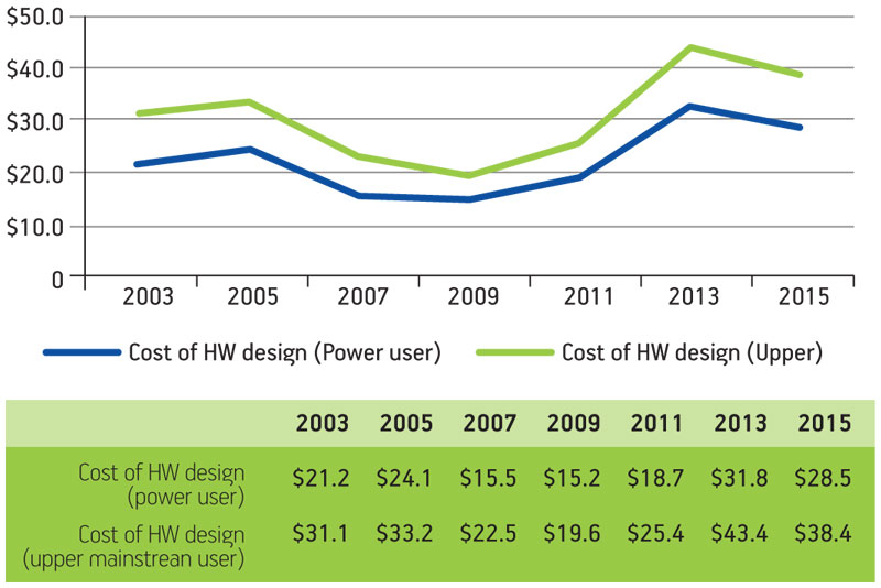
Figure 3
EDA revenue by user category in $M.
That hasn’t been good news for the EDA vendors that relied on the upper mainstream for most of their revenue. Cadence Design Systems has been the most obvious one to suffer. So let’s drill down a little into the issues surrounding design cost (Figure 4).
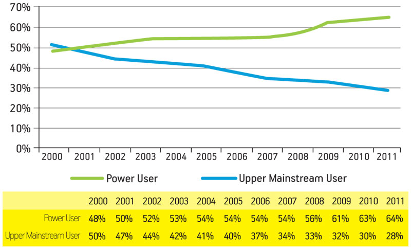
Figure 4
Cost of design by user category.
By 2003, the ITRS was reporting that the cost of an average high-end design flow at an upper mainstream company had almost reached a point where it was $10M more expensive than the cost of designing the same SoC on a power user’s flow.
Obviously, the upper mainstream designs had become uncompetitive and those companies consequently faced two choices: either upgrade to a power-user flow or reduce costs by getting out of the implementation portion of the design flow. The military vendors chose to upgrade and are adding to the revenue that the power users are spending with the EDA vendors. Automotive is also in the process of upgrading. On the consumer side, however, it is a different story. There, Nokia is a prime example of a company that has gotten out of the implementation business.
Ideally you would like to follow the Nokia path and restrict your design work to the ES level using an RTL handoff. Unfortunately, we have yet to come up with a silicon virtual prototype (SVP) that is reliable enough for, as it were, a hands-off handoff. There is still a lot of work that needs to be done by the semiconductor vendor (or design house) to make the hand-off work. That means that most of the consumer companies are still doing the RTL implementation and handing off at the gate level.
However, once SVP technology is perfected, upper mainstream companies will switch from buying RTL tools to purchasing ESL tools. As a result, the SVP will become a major ESL sub-application.
Some advice
Given all of the above, I would recommend that design engineers stop worrying about DFM issues. They are pretty much in hand and your design restrictions won’t impact you too badly. Once you do stop being concerned about all that, you will have more time to worry about what you will be designing after 2020. The switch from bipolar silicon design (current driven) to CMOS design (voltage driven) was painful enough. What happens if we end up with a non-silicon design fabric?
Gary Smith is the founder and chief analyst of Gary Smith EDA (www.garysmitheda.com).