Layout automation and simulation support DDR4 at lower system cost
The introduction of the DDR4 memory-bus standard will allow system designers to meet aggressive performance targets for their next-generation systems. But the changes required to support the higher datarates of DDR4 place stringent demands on the PCB designer.
The introduction of the DDR4 memory-bus standard will allow system designers to meet aggressive performance targets for their next-generation systems. The jump in performance and power efficiency is a big step from DDR3 — much larger than that of DDR3 from DDR2. The speed increases from 2133Mbit/s to 3200Mbit/s, with an extension allowing a doubling to 4266Mbit/s. At the same time, voltages reduces from 1.5V to 1.2V.
The changes required to support the higher datarates DDR4 place stringent demands on the PCB designer, particularly in systems that have to meet aggressive cost targets in order to be successful in the marketplace. The memory devices themselves will often be designed to go into lower-cost plastic packages that use leadframes rather than organic flip-chip packages. The higher inductance and capacitance of the leadframe design will leave less margin for the PCB designer, who will also need to find a way to accommodate the complex routing requirements of DDR4 buses on a low layer-count PCB.
Although protocols such as DDR4 have borrowed techniques from the lessons learned by designers of high-speed, low voltage-swing serial interfaces, the nature of the memory bus makes it more difficult to handle in PCB design than serial channels. The bus is bidirectional and can have multiple drops along it, known in the standard as the ‘fly by’ topology, an approach that was introduced to deal with the signal-integrity issues of the tree topology favored by the DDR2 standard. And, being a bus, it suffers from skew across the individual channels. The DDR4 protocol has a number of features designed to accommodate the timing problems of the fly-by topology, such as write leveling.
Reduced margins
The initial 3200Mbit/s form of DDR4 reduces the unit interval (UI) from 469ps to 313ps. The move to 4266Mbit/s, double that of DDR3, reduces the UI even further and channel interconnect skew and jitter already consume 50 per cent of the 2133Mbit/s DDR3 timing budget. Other factors, including the effects of impedance discontinuities, pin-to-pin capacitance variations, crosstalk and inter-symbol interference, mean that DDR4 designs are far more challenging to design, simulate and test.
It is not just the signal itself. The power distribution network (PDN) plays a major role in the design’s operating margins and signal integrity. The maximum ripple of the PDN falls from ±75mV for DDR3 to ±60mV for DDR4, making the design even more vulnerable to the effects of simultaneous switching noise (SSN).
The result is a requirement that attacks the problems of signal and power integrity at all levels. A solution is needed that employs a combination of system simulation and more intelligent PCB design tools that take into account the difficulties of designing with highly skew-sensitive buses.
The PCB designer dealing with buses such as DDR4 has to cope with potentially competing problems – to meet timing constraints as well as guarantee signal integrity for each trace. Constraint-based design evolved to help the layout engineer meet the timing requirements for each trace more quickly and efficiently. But traditional approaches to constraints management tend to focus on absolute targets that specific traces need to support. DDR4 and similar memory buses call for a more flexible approach because their timing and skew requirements are interdependent. Signals need to be matched against each other to ensure strobes are not misaligned with data. The reduction of the skew window with the move towards 4266Mbit/s buses makes this problem even more critical.
Dealing with constraints
Part of the issue is the way in which constraints are represented by the tool. When the constraints are primarily to do with individual signals, it makes sense to show the data in spreadsheet form as this matches the source of the constraints, which will be primarily datasheet descriptions or product specification documents. But the spreadsheet view makes it difficult for the designer to visualize how well a layout will meet the interdependencies of a high-speed memory bus.
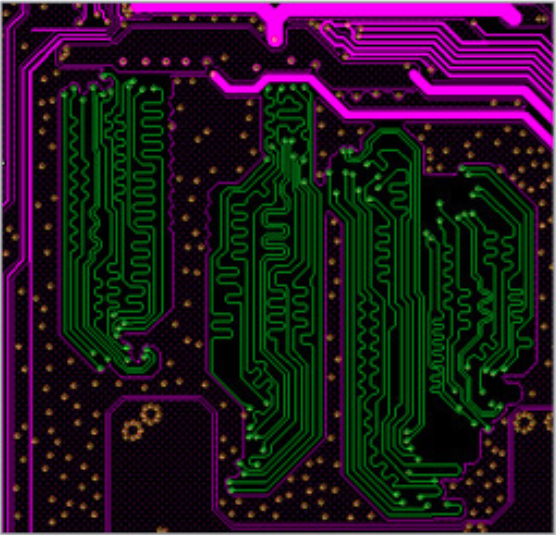
Image Automated routing in Allegro is used to insert bumps that normalise timing across channels
The Cadence Design Systems Allegro TimingVision Environment provides another way to view the effect of the constraints – on the design itself. An embedded route engine evaluates complex timing constraints and interdependencies among signals and color-codes their status. A green trace meets its targets, a trace is marked red if it is too short relative to those that meet their constraints and yellow if too long. This provides the designer with instant, usable feedback on how traces need to be altered to meet their skew requirements.
In many cases, the solution is not to meet the minimum timing constraint, as it may be practically impossible to meet that target without increasing PCB layer count, but relax the shortest paths. The Auto-interactive delay and phase tuning features of Allegro provide the tool with the intelligence needed to adjust traces so that they meet the application’s targets. Phase tuning ensures that each differential pair is matched correctly, an important step before moving onto delay tuning across bundles of differential pairs.
The next step is to ensure that the resulting layout meets its signal- and power-integrity targets as well as core timing. Interference and other sources of signal loss may call for certain traces to move into the inner layers of the PCB. Simulation using the Sigrity suite provides the necessary information to drive those decisions. The auto-interactive routing modes within Allegro ensure that the changes can be made simply and efficiently.
Capture the entire signal path
It is vital that signal integrity take into account all aspects of the signal path – which means evaluating everything from the chip I/O buffers through the package into the PCB and on to the receiving I/O buffer. Sigrity allows the engineer to extract all of the key parameters and parasitics for a design, including the package’s signal redistribution layer, PCB effects and connector attributes. A hybrid solver in the Hybrid SI technology models the signal, power, and ground interconnect information needed to judge how well the signal path meets signal and power integrity requirements.
The SystemSI tool performs the judgment by using the interconnect models and running simulations of data patterns to see how well the bus will meet bit error-rate targets across a range of scenarios through to worst-case conditions such as all data lanes changing state from one cycle to the next.
Advanced models of the I/O cells written to the IBIS Algorithmic Modeling Interface (AMI) allow for exploration of equalization techniques such as pre-emphasis that are required to accommodate high-speed interfaces with low voltage swings. These techniques now used on memory interfaces have been successfully deployed on serial interconnects. As a result of this end-to-end support, the combination of Sigrity and Allegro tools allow designers to meet both high-performance and low-cost targets.