Eliminating iterations in gigahertz ASIC handoff
How Cisco eliminated iterations in the ASIC handoff of a gigahertz networking chip by using physically aware synthesis
Working at advanced geometries brings timing closure challenges that make it difficult for design teams to complete their projects on schedule. For better predictability and to avoid time-consuming iterations with the ASIC vendor, users need to gain visibility into place and route issues before handing off the design. This article describes what the Cisco ASIC design team did to meet an aggressive timing goal. It highlights the flow the team used to gain visibility into physical implementation issues upfront. This flow enabled the team to meet its performance, cost and schedule requirements and eliminated iterations between Cisco and the ASIC vendor.
Cisco’s next-generation switch
Cisco’s annual Visual Networking Index projects annual global IP traffic to double by 2017, [source: Cisco Visual Networking Index: Forecast and Methodology, 2012-2017, May 29, 2013] . A significant part of this growth in traffic results from the proliferation of mobile and smart devices. By the end of 2013, the number of mobile-connected devices will exceed the number of people on Earth.[source: Cisco Visual Networking Index: Global Mobile Data Traffic Forecast Update, 2012–2017, February 6, 2013]. To meet current and future network traffic requirements, the network switch, the core of all networks, has to provide data centers with high-speed and low-latency connectivity.
While Cisco’s switch fabric meets current market requirements by implementing critical functions on multiple ASICs, the next-generation fabric must scale to provide higher network speeds, lower latency and greater port density for customers deploying virtualized data centers, where every microsecond counts. To meet the technical requirements, while minimizing impact on area and power, our design team elected to implement the core functionality on a 28nm ASIC. The package, board and ASIC design were scheduled concurrently to meet an aggressive product schedule.
ASIC handoff flow for the switch fabric design
Cisco decided to use the ASIC handoff model and collaborate with the vendor on the floorplan and timing closure. In this model (Figure 1), Cisco hands off a netlist to the ASIC vendor at the following stages in the development cycle:
- Initial exploration – completed interfaces and memory definition, used by the vendor to generate the initial floorplan
- Trial – 99% of the design is complete, functionally correct, clear of congestion and meets timing
- Final – Last run prior to handing off netlist for physical implementation.
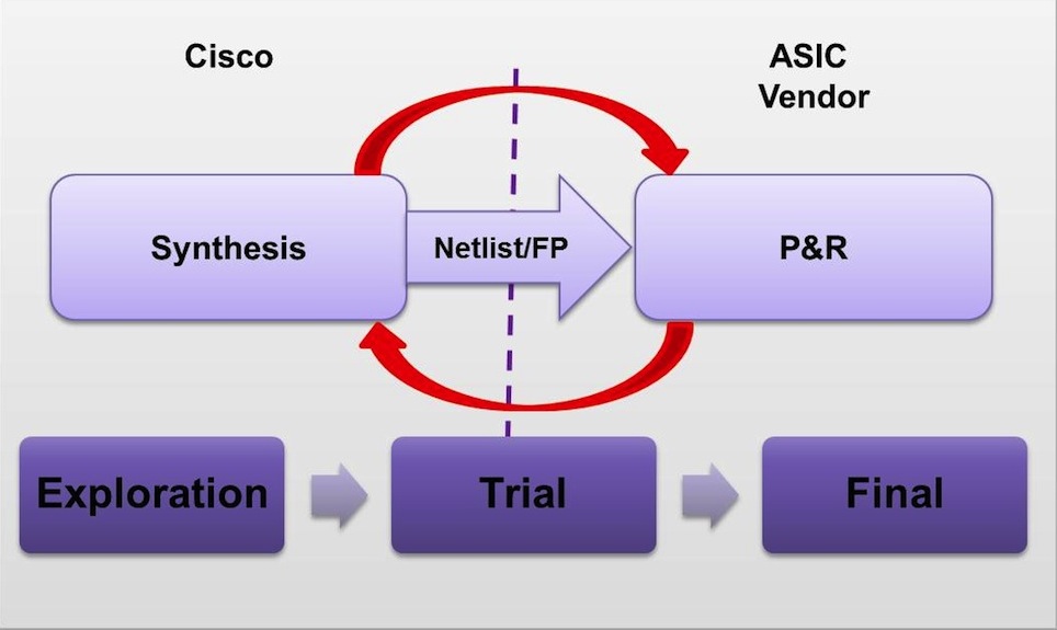
Figure 1 ASIC flow – iterations with ASIC vendors impact product delivery schedule and cost (Source: Synopsys)
The key requirements for Cisco when working with a vendor on the hybrid model were: timing predictability in synthesis; that the area stayed within the required limits; and that the design was free of congestion.
Design overview
The design includes high-density and high-speed memories, 7.5 to 15 Gbit/s SERDES, and a core clock rate of 1GHz. There is a 1.6Kbit-wide bus at the top level that carries data from the multiple-instantiated port blocks to the central crossbar. The critical block SC_PORT, shown in Figures 2a and 2b, gets instantiated multiple times. Optimal placement of macros and I/O pin locations are key to achieving performance for the top-level bus that routes to all the SC_PORT blocks.
In addition to meeting the 1 GHz timing requirement for SC_PORT, we also had to optimize for area and power. Any increase in area and gate count would not only have an adverse effect on power and floorplan, but also impact the package and board design. This, in turn, would negatively impact design cost and schedule.
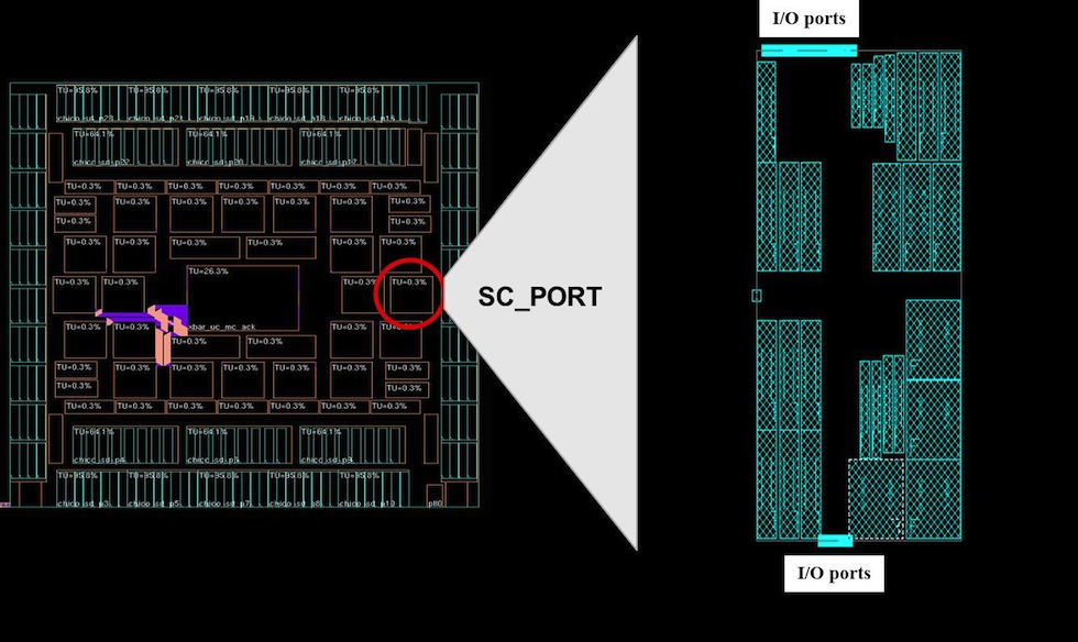
Figure 2 Chip floorplan with the details of one instance of SC_PORT (Source: Cisco)
Design challenges
The main challenge our design team faced was closing timing at 1GHz with an uncertainty margin provided by the ASIC vendor. Since we knew it would be difficult to meet timing requirements and that every picosecond mattered, the RTL was structured to minimize logic depth. After meeting timing in synthesis with the vendor’s margin requirements, the netlist with floorplan was handed off to the vendor for quality checks prior to physical implementation.
A few weeks later, the ASIC vendor reported they were unable to meet timing and were seeing routing congestion and increased gate count during physical implementation.
Achieving timing closure with Design Compiler Graphical
Our design team was under tremendous schedule pressure. We needed a synthesis tool that would account for physical effects, give us early visibility into physical implementation issues and address congestion. So we decided to use Synopsys’ Design Compiler Graphical, shown in Figure 3.
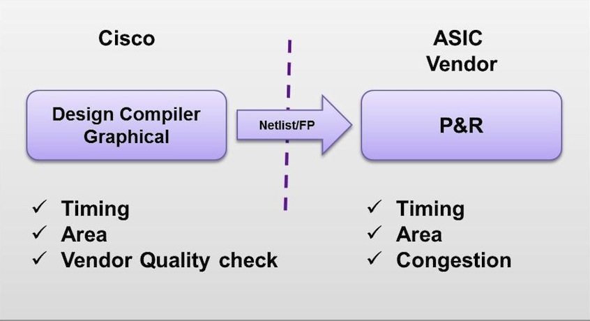
Figure 3 Design Compiler Graphical eliminates iterations with the ASIC vendor (Source: Synopsys)
Design Compiler Graphical extends DC Ultra topographical technology by applying additional physical optimization techniques, and considers small-geometry effects such as coupling capacitance for accurate delay modelling. It identifies highly congested areas in a design and performs congestion optimization to generate a routing-friendly netlist. Design Compiler Graphical uses technology shared with IC Compiler to take these physical effects into account to achieve superior quality of results. The innovative optimizations work with place-and-route technology to deliver faster timing on high-performance designs. They create a better start for physical implementation and accurately model small-geometry effects, bringing synthesis timing and area results to within 5% of layout.
After completing synthesis with Design Compiler Graphical, the netlist was run through the default IC Compiler placement flow. Design Compiler Graphical timing results were within 5% of IC Compiler. We were now able to see the real timing violations. The improved timing correlation helped us focus RTL changes for failing paths. With these changes, we achieved 16% faster timing, a design free of congestion, and 2% timing correlation with IC Compiler. We had met the 1 GHz target frequency with the vendor’s margin requirements. This netlist was handed off and the ASIC vendor was able to close the design without any more iterations.
For the Cisco gigahertz switch fabric ASIC, Design Compiler Graphical’s advanced optimizations generate a netlist free of congestion, with faster timing and predictable results during synthesis.
Conclusion
As design complexity grows, RTL designers need to gain visibility into physical issues to reduce iterations between synthesis and physical implementation. Design Compiler Graphical’s advanced synthesis optimizations, working with place and route technology, enabled the Cisco design team to meet timing, schedule and cost requirements. Better predictability, as well as insight into physical implementation challenges, helped the design team focus on real issues before handing the netlist off to the ASIC vendor. The netlist, optimized for timing, area and congestion, provided the ASIC vendor with an excellent starting point for physical implementation and so eliminated expensive iterations.
Venkataraman Srinivasagam is hardware engineering technical leader at Cisco
Hitesh Patel is product marketing manager at Synopsys