Quantifying returns on litho-friendly design
By the time a serious lithography-related problem is identified at the fab, it is too late in the design process to make simple layout changes. To avoid or reduce design delays, Infineon Technologies uses lithography simulation to detect weak points in a layout and analyze the effect of lithography on the design’s electrical performance. Its engineers can then implement any required adjustments early in the design flow.
Low k1 photolithography processes, increasing design complexity, and decreasing feature sizes significantly increase the challenges in applying reticle/resolution enhancement technologies (RETs) to nanometer-scale designs (Figure 1). The result has been higher silicon failure rates caused by mask rule constraints, fragmentation, modeling, metrology errors, and more besides. If a serious lithographic problem creates a non-functional chip, tapeout (and consequently chip delivery) can be delayed.
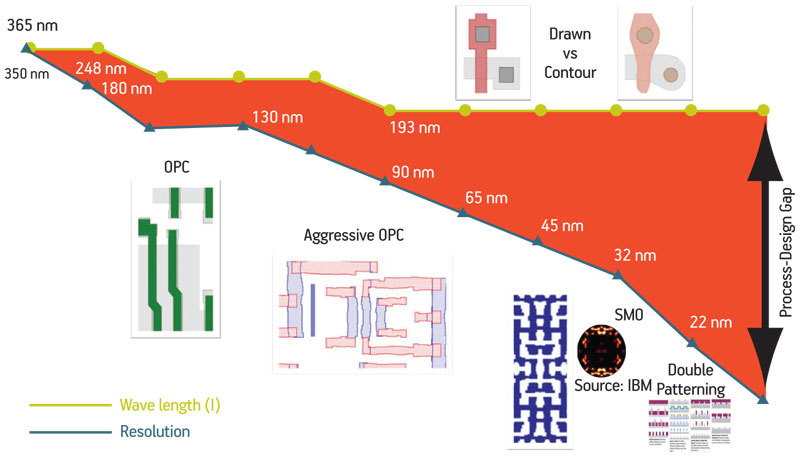
Figure 1
Growing gap between native resolution of photolithography technology and
target feature size required for nanometer designs. Source: IBM
Because each RET has its own layout limitations, some configurations are not easily combined in a specific RET recipe. These ‘unfriendly’ configurations are not only more vulnerable to process variation, but also slow down product yield ramp because they require diagnostic analysis and redesign.
Recommended design rules based on lithography knowledge help designers avoid sensitive configurations, and special tools let the fab perform post-OPC verification to identify printability issues before sending the layout to a mask house. But, despite these aids, at 45nm, designers need specific feature printability knowledge to create “litho-friendly” designs.
Existing optical proximity correction techniques (OPC) are not enough and there are two main challenges.
1. Designers are generally not familiar with lithography terms like ‘process window’, ‘slope of aerial image’ and so on.
2. A meaningful hotspot check requires a full sequence of RET data manipulations, such as selective biasing, sub-resolution assist feature (SRAF) generation, and especially OPC, before the optical rule checking (ORC) results become visible to the layout designer.
New tools enable designers to incorporate lithography process knowledge into their existing design flow. Infineon uses Calibre LFD, which works with a foundry litho-friendly design (LFD) kit to enable the designer to gauge the response of the layout to a given RET process, and then correct those configurations that mostly likely to fail during manufacturing (Figure 2).
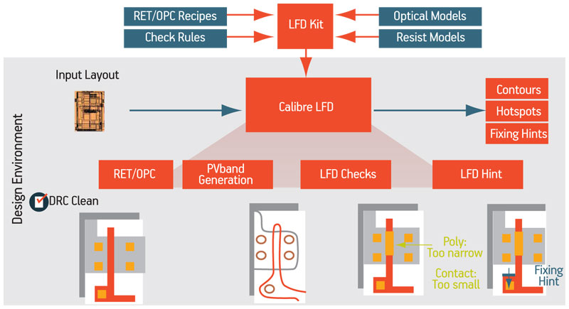
Figure 2
Calibre LFD flow. Source: Mentor Graphics/Infineon Technologies
Litho-friendly design at Infineon
Standard cell library optimization
Infineon has developed an interactive standard cell design flow in which layout engineers select the cell, layers of interest, and (optionally) specific process conditions (Figure 3). The Calibre LFD tool automatically applies RET/OPC; performs a process window simulation to obtain process variation (PV) bands; and checks the respective specifications (e.g., minimum width or spacing).
Figure 3
Infineon interactive design flow for library cells. Source: Infineon Technologies
The results are a GDSII file containing target and post-OPC layers, PV bands, and an ASCII database containing verification results with LFD errors and scores. Based on the errors, the layout engineer can start an inspection and remove printability issues.
The Infineon flow can be used to interactively analyze and improve single cells immediately, or analyze entire libraries to detect troublemakers in a specific library version, or analyze a real layout clip.
Standard cell library results
Running Calibre LFD on standard cells, Infineon identified multiple potential hotspots. Figure 4 (p. 44) shows a layout bridging hotspot that was found. Fixing guidelines (removing 5nm from each side) not only eliminated the bridging, but also meant that the PV band no longer showed a spacing violation.
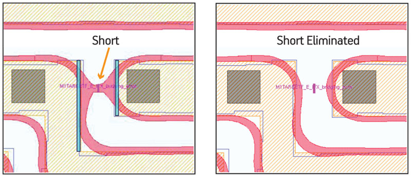
Figure 4
Lithography simulation finds a bridging hotspot. Red lines show the PV bands. Pink marker text shows the hotspot. Source: Infineon Technologies
The flow uses the mean width of the regular PV band to compare the sensitivity of a layout or a cell library by performing multiple process window analyses with different process models. In Figure 5, the higher value of the effective (mean) width of the PV band in Process 1 indicates that Process 2 is a better choice.
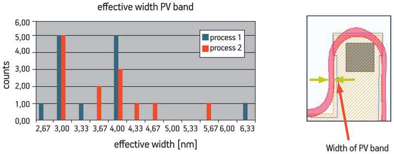
Figure 5
Mean width of the regular PV band is used to compare the sensitivity of a layout to two different processes. Source: Infineon Technologies
Litho-aware transistor parameters extraction
Infineon’s parameter extraction flow (Figure 6) is based on a LFD methodology from Mentor Graphics. We extract channel lengths of the MOSFET devices as gate critical dimensions (CDs) from the poly silicon over active layer. To obtain realistic gate CDs, layout polishing and RET methodologies are applied just as for a typical LFD analysis.
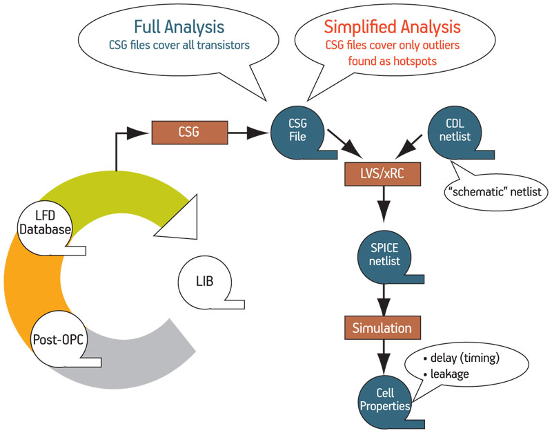
Figure 6
Two different analysis options for gate CD extraction from print contours. Source: Infineon Technologies
Using contours and PV bands created during the Calibre LFD run, we extract and re-emit device parameters using a contour simplified gate (CSG) convolution. The subsequent extraction flow (LVS/xRC) allows us to generate a SPICE netlist that represents a schematic netlist with updated channel lengths.
For full analysis, we extract the parameters of all transistors. For a simplified analysis that runs analog-to-hotspot detection, only the outliers (i.e., transistors with gate CDs deviating more than a specified threshold from the target value) are written to the error database. To support this alternative, the extraction flow is configured so that the SPICE netlist is filled from drawn dimensions if no channel lengths from LFD have been written out. This type of flow allows the designer to easily filter out critical transistors that may require improvement.
Two different checks are needed to support the analysis of across-chip linewidth variations (ACLV) and full process window variations. Figure 7 shows a schematic drawing of the poly silicon (red) over active area (light blue). The red line indicates the print contour at nominal process conditions, and the dashed line indicates the effective gate. We extract five different parameters for each device-under-test (DUT): the minimum and maximum gate length, its effective gate length and width, and the drawn channel length.
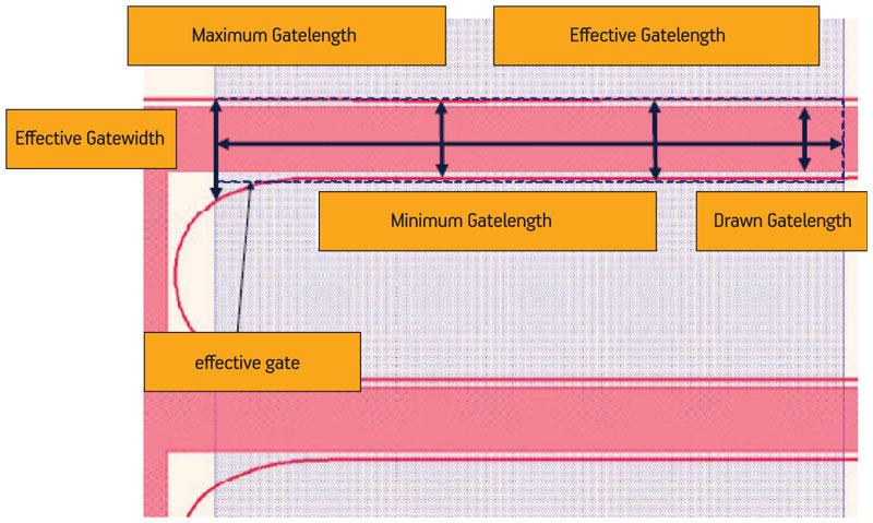
Figure 7
Setup for a check for extraction from the nominal print contour. Source: Infineon Technologies
The schematic drawing in Figure 8 describes the extraction over the process window. The purple band represents the device’s PV band. We extract four different parameters for each DUT: the effective gate length of the inner PV band (MinimumGatelength); the effective gate length of the outer PV band (MaximumGatelength); the average between effective gate lengths of the inner and outer PV bands (AverageEffectiveGatelength); and the drawn channel length of the DUT (DrawnGatelength). The average effective gate is indicated by the dashed line.
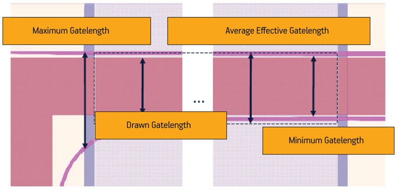
Figure 8
Setup for extraction from the process variability bands. Source: Infineon Technologies
Transistor parameters extraction results
We found that at 65nm, the ACLV values and maximum gate lengths over the process window are very close to each other (i.e., taking into account the lithographic process window, the gate length can only decrease). An average gate length over the process window is always smaller than the nominal or target value, and the distribution is always asymmetric with respect to the target. This behavior can be explained by the fact that the process used is limited by defocus.
The ACLV values are spread over a parameter range of about 3nm. The spread of the values over the process window is about 7nm wider, since an additional spread in the magnitude of twice the width of the PV band is applied.
At 45nm, the ACLV values are well centered within the process window values. This process apparently is not limited by defocus. Lithographic parameter variations within the specified range can lead to larger effective gate lengths, as well as smaller gate lengths.
Looking only at the spread of ACLV values, we could conclude that device properties for the 45nm library have a much higher percentage of uncertainty than those in the 65nm library. However, we should recognize that the process and process models for these two technology generations are most likely very different with regard to their maturity.
It is very important for Infineon to perform this analysis and reduce the ACLV metrics, as they directly impact timing results and power consumption. Tight variability control improves the predictability of the design performance compared to actual silicon results.
Full-chip optimization
Full-chip lithography simulations are normally impractical because of their long runtimes and the large number of CPUs required. However, Infineon can run full-chip simulations efficiently by filtering for candidate hotspots using a database of layout structures identified by the fab as potentially problematic patterns in specific contexts. You can run regular simulations on these areas to identify real hotspots. We also customize this filter to further improve the runtime by, for instance, excluding cells that have already been verified.
Full chip results
Our analysis of MAPLE, an Infineon 65nm design prototype, revealed minimum spacing routing issues in M1. Using a routing test case prototype (a very small standard cell design) that allows for full-chip analysis in various layout configurations, we investigated whether those routing issues could be resolved. Among the routing layers, M1 is particularly critical, due to the strong interference between the interior of the standard cells and inter-cell routing. This interference leads to a great variety of layout patterns and a higher tendency toward lithographic difficulties. For that reason, Infineon expected to see minimum spacing issues in the MAPLE prototype similar to those found in the test chip.
Even using DRC settings above minimum spacing in the router, Infineon identified a large number of lithography hotspots. As expected, when routing with the smallest DRC spacing, a significantly higher number of such hotspots were observed when compared with the use of larger spacing.
Benefit/value proposition of LFD to Infineon
Standard cells
Infineon considers LFD-cleanliness to be a sign-off criterion for new libraries. The company used Calibre LFD to detect lithographic hotspots in existing DRC-clean libraries, and this allowed it to fix errors before product release.
Additionally, because Calibre LFD is seamlessly integrated with all major place and route tools in the market, Infineon can evaluate different routers using the same libraries and settings, comparing those routers with regard to their litho-awareness.
Full chip impact
By using only LFD-clean components to create a production chip, Infineon discovered that full-custom macros created independently and layout-generated by the routing tool are potential sources of chip-level lithographic problems. The recommended practice at Infineon is to pre-characterize all blocks that go into a product well before actual tapeout. If we detect lithographic hotspots in full-custom macros, the macro owner has to fix the problem and deliver a lithographic-clean macro.
If we detect a lithographic hotspot in a generated layout, we analyze the problem to determine its root cause. In higher metal layers, routers can generate lithographic-unfriendly structures that challenge the RET recipe. Through the integration of place and route with LFD analysis, you can institute an automatic repair system to eliminate such hotspots in a post-processing step. You can tweak the RET setup, but we avoid doing this unless the error is a clear OPC defect triggered by an unusual layout configuration.
It is even harder for tools to generate a LFD layout in layers that contain a mixture of predefined features (e.g., a standard cell geometry) and router-generated layouts, due to the high density found in those layers.
Detected lithographic hotspots arise primarily from an interaction between cell and routing geometries. Infineon has observed problematic configurations such as ‘line end in U-shape’ and complex geometries rich in jogs (e.g., by placing double-cut vias). For such mixed layers, a short-term solution is hard to implement. A repair tool does not have much empty space to optimize the layout. Potential solutions include the use of blockages, the waiving of some double-cut vias, or even the exclusion of specific cells.
These examples demonstrate that the best approach is to address potential lithographic hotspots as early as possible. Performing incremental block-by-block analysis well before an actual tapeout saves time, as you address and solve all relevant problems before volume production. We have also set up countermeasures (such as automatic repair) as fall-back solutions. The business value of litho-friendly design technology is visible in volume production achieving confirmed high yields.
Kai Peter and Reinhard März were members of an Infineon Technologies team that introduced litho-friendly design techniques for use in the design flow for library cells, full custom macros and semi-custom layout starting at 65nm. Reinhard recently joined Intel Mobile Communications as part of Intel’s acquisition of Infineon’s Wireless Solutions business.
NanGate Inc
155A Moffett Park Drive, Suite 101
Sunnyvale
CA 94089
USA
T: +1 408 541 1992
W: www.nangate.com
NanGate A/S
Smedeholm 10
Herlev
DK-2730
Denmark
T: +45 4452 1400
W: www.nangate.co
