Creating a new paradigm for circuit verification
Layout verification has become a major contributor to delays in design delivery. This has been growing in impact for many reasons, including increases in design complexity, design sizes, number and types of devices, number of polygons, and more complex measurements and parameter calculations. In parallel, the number of verification operations has not simply increased, but become more complex because of the needs to verify designs against new and expanded performance and operational requirements, increased context sensitivity, and additional manufacturing operations such as multi-patterning. As you can see from this list, verification complexity applies to all aspects of the verification process—physical verification, circuit verification, reliability analysis, and DFM closure.
If we delve into verification delays a bit more deeply, we find that one significant factor in the overall turnaround time of the verification cycle is design readiness. Designs that are in the early stages of implementation and assembly are often referred to as “dirty”, meaning they contain many issues that exist only because of the incomplete state of the design. When a designer tries to run a full signoff layout vs. schematic (LVS) verification cycle on a dirty design, the result is typically thousands, even millions, of errors. Because there is no way to separate out true errors from those caused by the immature state of the design, designers are forced into time-consuming, hardware-intensive debugging cycles. Even if these early LVS runs eventually result in a very short final LVS cycle, the total time consumed has usually already delayed delivery schedules.
Unfortunately, designers do not have the luxury of time in today’s fast-moving markets. To meet aggressive time-to-market schedules, designers are often forced to start chip integration before individual blocks are complete or even available. Design and verification activities simply have to take place in parallel, because companies cannot afford to wait until a chip is complete and DRC-clean before running full-chip LVS verification.
But what if you could get rid of many of those systemic early-stage errors quickly and efficiently, before getting bogged down in seemingly endless analysis and debugging cycles? That’s the idea behind early-stage verification, a new approach that uses an intelligent process to rapidly examine dirty, immature, and early-stage designs to analytically discover specific types of systemic LVS violations, and fix them earlier and faster. The Calibre nmLVS-Recon (short for reconnaissance) solution developed by Mentor, a Siemens business, uses innovative options for data partitioning, data re-use, task distribution, and errors management to help designers achieve faster layout vs. schematic (LVS) iterations on dirty designs. Verification engineers can use the shorter, faster Calibre nmLVS-Recon process to interactively and iteratively find and fix these types of violations until the design is ready for full-chip signoff LVS iterations.
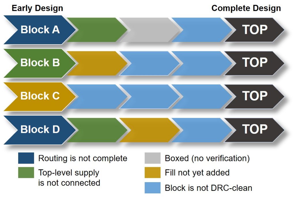
Let’s take a look at a simple example of a chip containing four blocks, each at a different stage of readiness. As the chip moves from the dirty stage to full-chip LVS-ready, each block evolves at a different pace to different levels of completeness (Figure 1).

Figure 1. Design and verification activities often happen in parallel, with different components of the design in different stages of readiness (Mentor)
In a traditional LVS verification flow, engineers run the LVS signoff tool on a design database over and over, each and every time the database is modified, a block is edited, or an error fix is applied. Each LVS iteration validates a list of circuit verification requirements, starting from connectivity extraction, device recognition, establishing soft connections and reporting their conflicts, open/short paths isolation, electrical rule checking (ERC), advanced device parameters computation, and detailed layout versus schematic comparison.
Unlike design rule checking (DRC) or other physical verification that evaluates shapes and geometries, one of the unique aspects of circuit verification is the heavy connectivity dependency and the complex hierarchical context required to establish the base for fully-executed LVS verification. These essential conditions make it nearly impossible to partition or break down a design into smaller sections. Even if a team could spend time scripting its way through (and supporting and maintaining) customized home-grown flows, there would still be no way to guarantee these flows would provide accurate results.
The Calibre nmLVS-Recon solution introduces a more intuitive approach to early-stage circuit verification to execute only those checks required to solve the highest-priority issues, while also providing fast, interactive feedback that enables designers to quickly analyze, fix, and verify these selected design issues. The essential elements of the process include:
- Categorization: Focusing on specific types of violations
- Prioritization: Addressing the most impactful errors first
- Task Distribution: Enabling different teams to focus on a specific set of design issues simultaneously
- Partitioning: Splitting data for easier debugging and root cause analysis
- Data Reuse: Incremental execution on existing database and disk files
- Interactive approach: On-the-fly editing to verify resolution, consolidate fixes, and speed up the debugging cycle
What is a high-impact circuit verification problem in an early-stage design? Our analysis of multiple projects in their very early stages revealed that an average-sized dirty design has around 30k short paths that must be analyzed and fixed by designers. Teams reported spending up to 80% of their early-stage verification time analyzing and fixing shorts, sometimes taking weeks to debug complex shorts.
Why are shorts so hard to find and fix? A complex short can extend throughout an entire chip when it involves huge nets or a power/ground grid short. A single short can be composed of many short paths, all of which must be analyzed to ensure the issue is fully resolved. Shorts and opens in the design impact the accuracy of other analysis performed in typical circuit verification stages (such as ERC or floating nodes inspection) that typically pertain to connectivity dependencies and require full hierarchical context analysis.
For all those reasons short paths analysis, isolation, and debugging is the first use model available in the Calibre nmLVS-Recon solution. This short isolation (SI) use model focuses solely on short isolation and short paths debugging, executing only those steps of selective connectivity extraction that are needed to construct the required paths for short isolation analysis. Built-in configurations allow designers to focus on those areas in the design that are of particular interest:
- Layer-aware SI partitioning divides the design into layer groups to analyze shorts on specific layers of interest
- Back-end-of-line vs. front-end-of-line layers
- Top-level metal routing vs. block-level routing
- Incremental segmentation per metal pairs
- Net-aware SI focuses on analyzing critical shorts by targeting a design’s most impactful nets first, as determined by the size of the net and how it propagates throughout the chip.
- Focus on specific net types (power/ground, signal/IO, others)
- Sensitive net isolation
- Prioritize impactful nets analysis first
- Custom SI enables customizable input for even more precise short paths analysis and concise per-net iterations
Here’s an example of the Calibre nmLVS-Recon short isolation process:
- An SoC engineer initiates the Calibre nmLVS-Recon SI process, focusing on the layers constructing the power/ground paths. The Calibre nmLVS-Recon process automatically determines which circuit verification requirements must be executed for maximum efficiency.
- The resulting database is shared with a team of designers who, in turn, run the Calibre nmLVS-Recon SI process on power/ground nets, each selecting a specific set of layers.
- The team uses the Calibre RVE interactive SI features to quickly isolate the short on each of the designated layers.
- For each short, a designer edits the database on the fly, running multiple iterations of Calibre nmLVS-Recon SI verification to ensure the short is fixed for the assigned layers.
- After fixing the shorts for all layers, the design edits are approved and saved.
- The team selects another set of layers and repeats the process until all power/ground shorts are fixed.
- The team repeats the Calibre nmLVS-Recon SI process for signal nets.
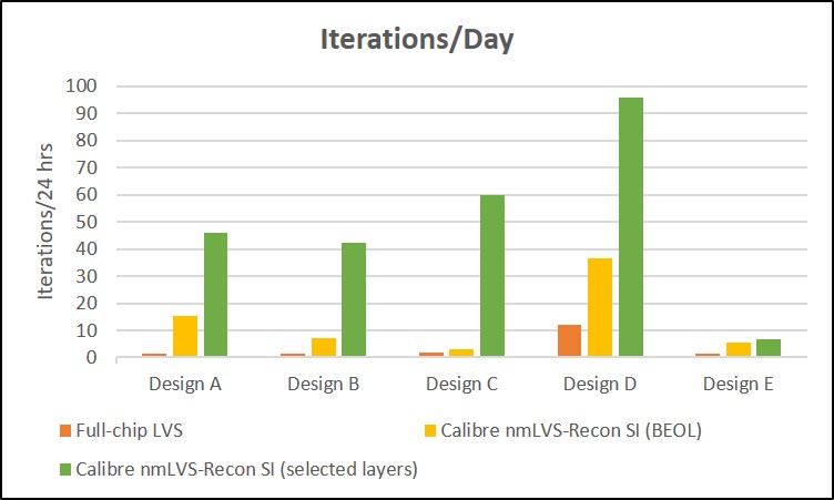
Companies leveraging the Calibre nmLVS-Recon solution for early-stage SI analysis have experienced up to 30x faster iterations, with leaner hardware usage. Figure 2 shows the iteration rates achieved for both BEOL and selected layers SI verification, compared to full LVS runs.

Figure 2. Using Calibre nmLVS-Recon, designers can reduce iteration runtimes and resource requirements while focusing on high-impact circuit errors in early stage designs (Mentor)
Looking ahead, the Calibre nmLVS-Recon use models will be expanded to include selective electrical rule checking (ERC, soft connectivity conflict analysis, and circuit/layout comparison). However, the goal remains the same: enable fast identification, debugging and fixing of selective circuit issues in dirty designs so teams move through early-stage circuit verification more quickly and efficiently.
Innovative verification options such as the Calibre nmLVS-Recon solution introduce a new paradigm for early-stage design circuit verification, providing intuitive and easy-to-use use models that enable design and verification teams to collaborate on dirty design verification more quickly and efficiently, without compromising their signoff flows, leading to an overall reduction in delivery schedules and time to market.
For more information, download the whitepaper Accelerate time to market with Calibre nmLVS-Recon technology, a new paradigm for circuit verification.
 Hend Wagieh is the senior product manager for Calibre circuit verification at Mentor, a Siemens Business. Her responsibilities include defining the product roadmap, business strategies, and associated new use models needed to grow the product line and increase market competitiveness for the Calibre nmLVS platform. Hend holds a degree in Electronics and Communication Engineering from Ain Shams University in Cairo, Egypt.

