Speed up design and verification with a smaller layout
 Dennis Joseph is a technical marketing engineer supporting Calibre interfaces in the Design-to-Silicon division of Mentor, a Siemens business. His primary focus is the support and enhancement of the Calibre DESIGNrev layout viewer. Dennis received an M.S. in Electrical and Computer Engineering from the University of Florida.
 Today’s large full-chip integrated circuit (IC) layouts can be very frustrating. Just viewing them requires powerful computers with substantial memory, and they are not always readily available. Even when they are, and even if you switch database formats to minimize loading time, you still have to wait for the full layout to load. Tick-tock.
But isn’t that just part of the job? Well, quite often, designers only need a portion of the layout for a particular task. When that is the case, not only do they have to waste time loading the full design, but they can also find themselves distracted by extraneous information. It is like going into a store for one item, only to find the store keeps all its products in one aisle.
This issue comes up often throughout the design and verification process. Computer-aided design (CAD) engineers may want to use realistic layouts to build their end-user design flows without the bulk of a full layout. System-on-chip (SoC) integrators may only want to view top-level routing, ignoring all the content within an IP block. Conversely, block owners may want to focus only on their blocks, with just the added context of viewing interconnects and top-level routing that crosses their blocks. Physical verification engineers may find that running design rule checking (DRC) at the full-chip level is too time-consuming, and produces too many results to manage effectively. Likewise, circuit verification engineers may be unable to quickly and effectively debug large power and ground nets that span most of the design.
Saving part of a full-chip layout as a separate layout allows engineers to focus only on the area that is relevant to the specific task at hand. By defining what parts they would like to keep (or what parts they would like to remove), engineers can create a smaller, more portable layout that they can view easily and use to run simulations more quickly. They can also more easily share these smaller layouts with colleagues.
But this is not always as straightforward as it appears. For instance, engineers often try to save a particular cell or layer as a separate layout, a common feature in many tools. Saving a block as a separate layout does not give block owners the context of what else exists around or on top of their block. As a result, the differences between different placements of the same block would not be captured. Saving specific layers may also result in an overwhelming amount of data to run simulations against and debug, especially for circuit verification engineers trying to debug large power and ground nets that span a chip.
Sharing coordinates for locations of interest is a commonly used technique in a team design environment. However, sharing only coordinates means colleagues are still forced to load the full layout themselves. More time wasted. Another option, sharing screenshots, may offer too much context to the recipient, who cannot disable specific layers to focus on a particular issue. Neither approach is ideal, as both typically provide either too little or too much context.
In all these cases, a better solution is to save particular regions of the full-chip layout separately. This allows engineers to create as much context as they want or need around the region of interest, and no more. Before they can do this, engineers must decide what that desired context is, and what is the best way of getting it. For instance, they may find it easier or more useful to include certain areas (“I just need these parts”) or to exclude certain areas (“I don’t need those parts”). By clearly defining their areas of interest, engineers can create a much smaller layout that they can use to run simulations and verifications more quickly, debug more effectively, and share more easily with colleagues.
Fortunately, EDA companies have stepped up with solutions that can help designers quickly and easily create their desired outputs. While the specific methods may differ between tools, the general capabilities are fairly similar.
Saving specific areas from a layout
Our first example is a simple use-case in which the engineer wants to include only a few specific areas, which can contain any number of cells or layers. Many layout viewers offer a function that allows designers to interactively define the regions of interest, as seen in Figure 1.
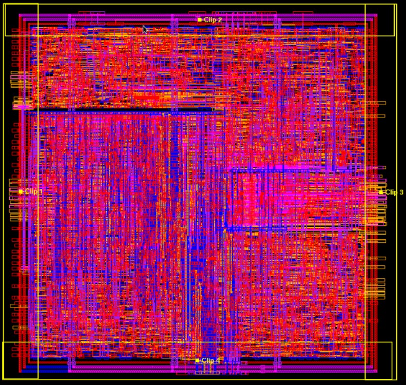
Once the desired areas are defined, engineers can save them as a separate layout. This output (Figure 2) can now be used for debugging or to share with colleagues. As you can see, this smaller version contains only the regions specified in Figure 1, allowing engineers to focus on their areas of interest.
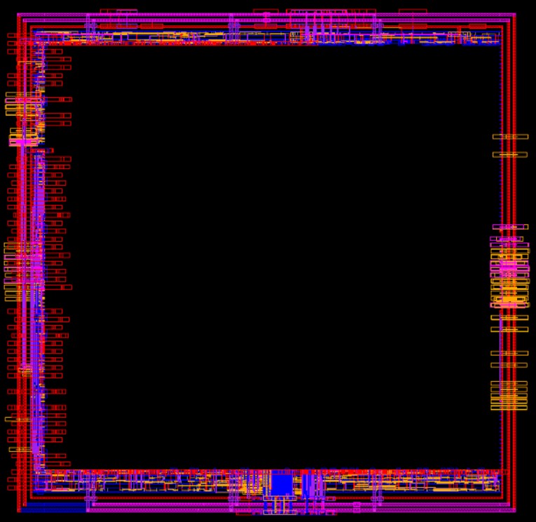
Figure 2. The selected regions are saved into a separate, smaller layout (Mentor – click to enlarge)
Although engineers can select as many regions as required in this manner to produce their desired layout, this approach only allow engineers to define the areas they want to keep. It may sometimes be easier to define areas of the original to remove instead.
Removing specific areas from a layout
If engineers want to define areas to remove, they will have to be familiar with their layout viewer’s capabilities. This process varies more widely across tools, and may not be available in all viewers. For this example, we are using the Calibre DESIGNrev layout viewer’s ‘filtershapes’ functionality.
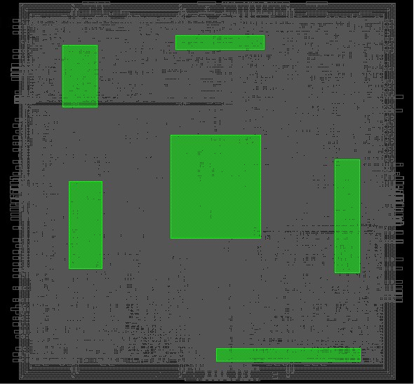
The first thing required is a filter layout that defines the regions to remove from the original. This layout can be the output of a batch tool (such as a DRC tool) or created interactively by drawing the regions of interest in the viewer. Figure 3 shows a filter layout containing multiple polygons that define multiple regions to remove from the original layout. These polygons are created on a separate layer and overlaid on the original layout; however, the polygons to be removed may be on any layer, or even on multiple layers.
Now the engineer creates a map file. This is a plain text file that explicitly defines which layers to remove from the original layout. The map file is needed to instruct the Calibre DESIGNrev layout viewer to selectively remove polygons on specific layers.
Once the filter layout and map file have been created, the Calibre DESIGNrev tool uses these together to execute the filtershapes functionality and create a layout that excludes the defined regions from the specified layers (Figure 4).
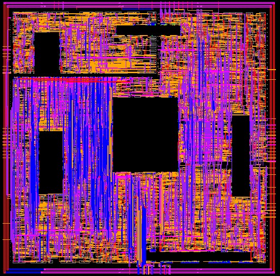
Figure 4: The output of the filtershapes command. The polygons in regions defined in Figure 3 are removed to create a new, separate layout (Mentor)
Conclusion
When only part of a large layout is of interest, saving a smaller, separate layout can reduce loading times and large memory requirements. This will help save a lot of frustration and confusion. Breaking a full-chip layout into smaller, more manageable pieces can help focus an engineer’s efforts. In a team environment, smaller layouts are also more conducive to sharing data between colleagues. EDA tools that provide automated functionality help engineers easily define the parts of a layout that are relevant to their specific application. By focusing more effectively on specific tasks, while avoiding the frustration of dealing with a large layout, engineers can become far more productive during debug. This helps to reduce the time needed to close physical and circuit verification tasks.
For more details about the Calibre DESIGNrev layout viewer and its filtering capabilities, download the white paper Splitting IC layouts for faster verification and debugging.