Automate P2P resistance checking for better, faster ESD protection
ESD has always been a major issue but with increasing densities and growing die sizes it is becoming a higher order concern. Automation and vizualization can help manage the task.
Performance reliability is a fundamental to market success. If you can’t depend on a chip to operate as designed throughout its expected product life, why would ever you buy it?
One of the rising challenges facing reliability is electrostatic discharge (ESD). Yes, that same spark that snaps your fingertips when you touch a doorknob is also an IC killer. Finding and eliminating causes of ESD in IC layouts has always been an essential part of circuit verification but growing die sizes and increasing transistor densities ICs have made it a critical task. Unfortunately, not only has ESD verification and debug become more difficult due to the complexity of large IC designs [1,2], but it is also requiring more computing resources (such as CPUs and memory) and longer runtimes. Not good for the bottom line. The good news? Innovative verification technology is helping designers protect both their IC designs and their tapeout schedules.
ESD event protection
An ESD event occurs when an unexpected electrical discharge occurs in a circuit. This discharge can leave the circuit susceptible to performance degradation over time or result in outright failure. To prevent ESD damage, circuits are designed with ESD protection devices and discharge paths to allow any excess current to safely drain off without affecting the IC circuitry.
To provide sufficient protection against an ESD event, IC designers must make sure that not only are ESD protection devices implemented properly, but also that the ESD discharge paths are efficient and robust. For example, one rule often included in rule decks is that the resistance of an ESD discharge path (which is the path between an ESD source (e.g., a physical pad) and its ESD protection device) must be less than a certain design threshold [2].
Figure 1 illustrates some typical ESD protection schemes and common ESD discharge paths [3,4]. In Figure1a-d, the I/O pad is protected by pull-up and pull-down diodes, an ESD resistor, and secondary ESD diodes. A power clamp is connected between the power bus VDD and ground bus VSS. In Figure 1e, a pair of back-to-back connected diodes are used to connect the ground busses VSSA and VSSB from two power domains.
![Figure 1. Common ESD protection schemes and ESD discharge paths (highlighted in green): (a) I/O pad and power clamp; (b) I/O pad and power pad; (c) power pad and ground pad; (d) ESD resistor and power clamp; (e) I/O pad and I/O pad [3,4] (Mentor)](https://www.techdesignforums.com/practice/files/2020/03/Fig1_ESD-schemes-paths.jpg)
Figure 1. Common ESD protection schemes and ESD discharge paths (highlighted in green): (a) I/O pad and power clamp; (b) I/O pad and power pad; (c) power pad and ground pad; (d) ESD resistor and power clamp; (e) I/O pad and I/O pad [3,4] (Mentor).
Checking ESD path resistance
Figure 2 shows a simple circuit design in which the I/O pad ‘INA’ should be protected by pull-up and pull-down diodes. Figure 2a is the schematic, showing INA connected to a pull-up and a pull-down diode. Figure 2b is the corresponding layout design. To ensure sufficient ESD protection on INA, designers must not only ensure that the pull-up and pull-down diodes are connected to the I/O pad and meet certain dimension requirements, but also that the resistance between the INA and the pull-up or the pull-down diode, respectively, is within the design threshold.
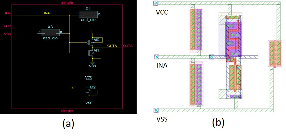
Figure 2. Simple circuit design with ESD protection on I/O pad: (a) schematic showing an I/O pad named ‘INA’ is connected to a pull-up and a pull-down diode, (b) corresponding layout design (Mentor)
We will use this simple design case to demonstrate how circuit verification engineers can check the resistances along ESD discharge paths and debug resistance violations, using the Calibre PERC reliability platform as our verification tool.
Most semiconductor foundries can provide their customers with foundry-supported Calibre PERC flows to check for ESD protections and multiple discharge path constructions in layout designs. Because the Calibre PERC platform is seamlessly integrated with Calibre layout versus schematic (LVS) rule decks, design companies do not have to write their own to check for common ESD rules (although they may write custom decks to check for unique internal ESD requirements).
The Calibre PERC P2P resistance flow first runs layout extraction based on the LVS rule deck to generate the device and connectivity information of a layout design. Using the resulting layout netlist, the Calibre PERC tool runs topology analysis to identify I/O, power and ground pads, and ESD devices. Based on definitions given in the rule deck, it then determines the source and sink (or pin pair) for resistance calculation (in Figure 2, this is I/O pad INA, and the pull-up or pull-down diode, respectively) and calculates the total effective resistance between each pin pair using simulation. Any pin pair with a total effective resistance value higher than a pre- defined design threshold is flagged as a violation.
In the simple design shown in Figure 2, the resistance between INA and the pull-down diode is approximately 15.8 ohms, which exceeds the given design threshold of 2.0 ohms. This measurement is flagged as a resistance violation. All violations are output to a results database, which is viewed and debugged using the Calibre RVE results viewer.
After loading the results in the Calibre RVE results viewer, designers can see the resistance violation is flagged, as shown in Figure 3a. Highlighting this resistance violation in the Calibre RVE display enables designers to use the Calibre DESIGNrev layout viewer to display a fly line between the source (I/O pad INA), and the sink, which is the pull-down diode, as shown in Figure 3b.
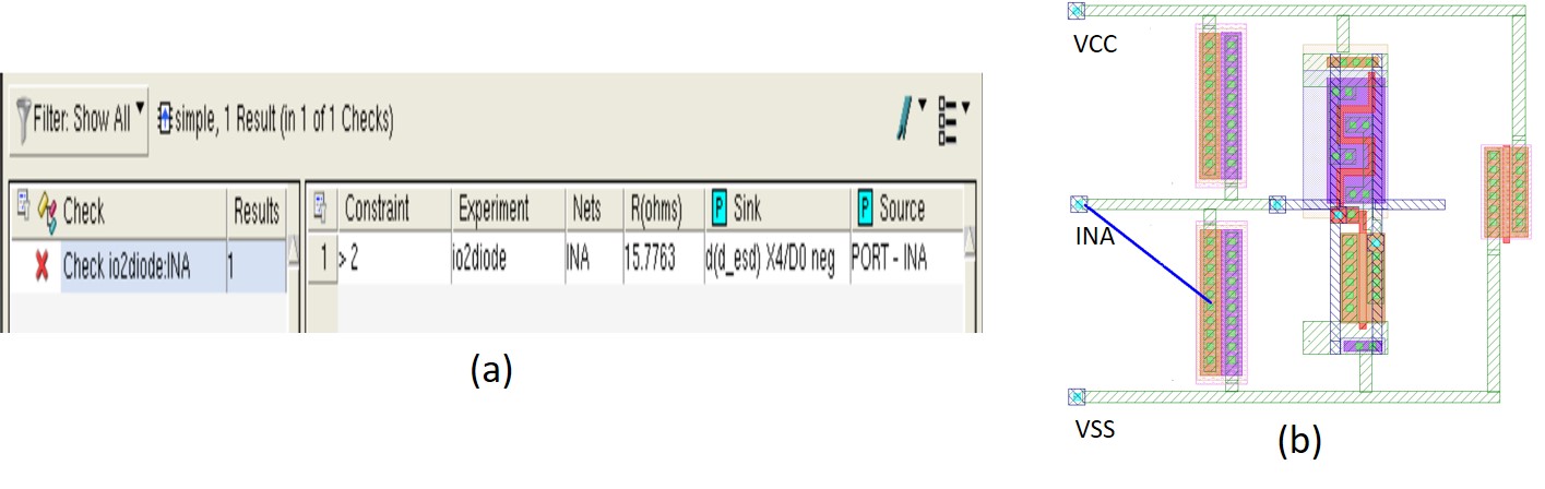
Figure 3. Displaying (a) resistance violation details in a (b) visual format helps engineers more quickly understand where resistance issues exist in an ESD protection path (Mentor)
In a large and complex layout design, however, merely knowing there is a resistance violation on an ESD discharge path does not give layout designers enough information to fix the violation. They must be able to quickly and accurately determine where in the layout changes should be made to reduce the total resistance of the ESD path.
Debugging resistance bottlenecks
The Calibre PERC platform generates debug information that can be used to highlight an entire ESD path containing a resistance violation in the Calibre DESIGNrev layout viewer. Designers can highlight all polygons on an ESD path, including metal routes and vias, that contribute to the total effective resistance exceeding a given design threshold, as shown in Figure 4.
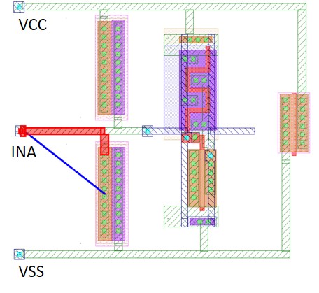
Figure 4. All polygon segments of an ESD path with a total resistance violation are highlighted (in red) in the layout viewer (Mentor)
Because the Calibre PERC flow also reports the percentage contribution of each metal and via polygon to the total effective resistance of an ESD path, designers can initiate the Calibre DESIGNrev colormap feature from the Calibre RVE results viewer to display different colors based on each polygon’s percentage contribution to the total effective resistance of an ESD discharge path (Figure 5). The polygon segments of the ESD discharge path between I/O pad INA and the pull-down diode are highlighted in different colors: Red indicates the highest percentage contributions, and blue the lowest percentage contributions. The percentage range of each color is shown in the layout viewer and can be adjusted to suit the preference of each user.
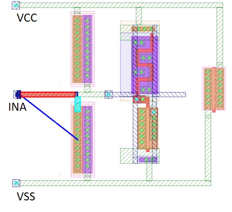
Figure 5. Polygon segments of the same ESD path highlighted in different colors, based on the percentage contribution of each polygon to the total effective resistance of the ESD discharge path (red indicates highest percentage contributions, and blue indicates lowest percentage contributions) (Mentor)
The polygon segments with the highest percentage contributions to the total effective resistance are usually the resistance bottlenecks on the ESD path. Being able to highlight these elements provides a useful visual aid when tracing an ESD path for possible layout issues and fixes, especially in a large and complex layout design (such as a full chip layout database). Colormapping allows layout designers to quickly identify the resistance bottlenecks along an ESD path and make necessary layout changes, such as widening metal routes or adding additional vias, that reduce the total effective resistance of the ESD path. It is especially helpful when debugging resistance violations in a large and complex layout design, where manually inspecting the layout for resistance bottlenecks is extremely difficult and time-consuming.
Summary
With advanced semiconductor process nodes, and the smaller transistor and interconnect feature sizes prevalent in leading-edge IC designs, finding and eliminating ESD problems quickly and efficiently is critical to ensuring the reliability of ICs while maintaining production schedules. Checking the resistances of ESD discharge paths in a layout to determine if they are within pre-defined design thresholds plays an essential role in ESD protection in IC chip designs. Utilizing an automated approach to detect and highlight these resistance violations within ESD paths for faster and more accurate debugging helps designers alleviate the difficulty and cost of detecting and eliminating potential ESD issues in today’s large and complex IC designs.
References
- Ille, et al., ‘Reliability Aspects of Gate Oxide under ESD Pulse Stress’, Proc. Of 29th EOS/ESD Symposium, pp. 328-337, 2007.
- Yan, ‘Ensuring Robust ESD Protection in IC Designs’, Mentor, a Siemens Business, 2017.
- EDA Tool Working Group (ESD Association), ‘ESD Association Technical Report’, ESD 0-01-14.
- Chang, Y. Liao, Y. Li, P. Johari, and A. Sarkar, ‘Efficient Multi-domain ESD Analysis and Verification for Large SoC Designs’, Proc. of 33rd EOS/ESD Symposium, pp. 1-7, 2011.
About the author
Derong Yan is a technical marketing engineer for the Calibre PERC reliability platform at Mentor, a Siemens business. His areas of expertise include SoC physical design and verification, reliability verification, and design automation. Prior to joining Mentor, Derong worked in multiple semiconductor companies, including Micron Technology and Intel Corporation. He holds a PhD in Materials Engineering from the University of Alberta, and received both his MSc. and BSc. from Shanghai Jiao Tong University. Derong can be reached at derongUNDERSCOREyanATmentorDOTcom.