Adding system-level, post-layout electrical analysis to HDAP design and verification
Adoption of high-density advanced packaging (HDAP) needs tools and supports to build designers’ confidence in the emerging technology.
High-density advanced packaging (HDAP) offerings from both outsourced assembly and test (OSAT) companies and traditional IC foundries are increasing in number and expanding in design options every day. However, it is unlikely that HDAPs will enjoy full commercial exploitation until these companies can assure the design companies of an acceptable yield and correct (as intended) functionality. This assurance, like that for ICs, will come from the availability of proven and qualified electronic design automation (EDA) tools and flows that can be used by the design houses to build HDAPs with the confidence that they are compliant with the foundry/OSAT requirements and recommendations.
My colleagues and I have discussed the need for an assembly design kit (ADK) that is similar in nature to an IC process design kit (PDK). This would allow for the provision of proven, qualified flows for HDAP design and manufacturing [1][2][3][4]. We have analyzed the need for assembly-level layout vs. schematic (LVS) verification of HDAPs [5]. Potential best practices for an assembly-level LVS process have been identified, including required inputs (data, formats, etc.), and the likely hurdles and potential errors have been highlighted [6]. There has even been discussion of how parasitic extraction (PEX) could be achieved for packages [7].
However, here is the reality for now. Although they depend in part on just how complicated an HDAP design is, not even package design rule checking (DRC), assembly-level LVS, and layout vs. layout (LVL) verification (die-to-package alignment, scaling, orientation, etc.) are generally sufficient to guarantee the correct functionality of an HDAP. While physical verification is a good start, achieving commercial success will require a much more comprehensive flow. Such a flow must account for a more in-depth, system-level electrical analysis, supported by expanded EDA tool functionality and fast, accurate, automated flows that ensure package designers can meet schedules and expectations.
What does a comprehensive electrical analysis look like for an HDAP design? For an analog-based flow, designers must be able to simulate all of the HDAP circuitry (including parasitics) to ensure the HDAP meets the designed performance specifications. For a digital-based flow, designers must be able to run static timing analysis (STA) on the complete HDAP system (again including parasitics) to ensure it meets the overall timing budget. To conduct post-layout circuit simulation (analog/RF) or STA (digital) for an HDAP, you must generate a system-level layout netlist that accounts for the overall system parasitics.
What does that mean in practice? For simplicity’s sake, we will stick with the example of a digital-based flow, but the concepts apply generally to both analog and digital HDAPs. In addition, we will refer generically to automated capabilities available from the growing set of EDA package verification tools and capabilities. We will discuss those tools in greater depth later.
System-level post-layout analysis for HDAPs
A clean start
Before beginning, you must ensure that the HDAP is LVS-clean (meaning all connectivity has been verified). Next, you must ensure that the HDAP layout netlist includes all the necessary components, as described below.
System-level connectivity
A system-level source netlist in the format required by STA tools (typically Verilog) must be available. This netlist is analogous to a schematic in the IC world and is generated using system-level connectivity tools. Like the IC schematic, this netlist is the ‘ideal’ netlist from a parasitics point of view, meaning the die-to-die and die-to-package connections are assumed to be ideal wires.
Die-level layout parasitics
You must have a parasitic layout netlist for each die in the HDAP. This is the easiest part, because these die have already been verified and taped-out by IC design teams, so the netlists should already be generated in the required format.
Package-level layout parasitics
You must generate a parasitic layout netlist for the package in the HDAP system. Typically, designers use a package-level PEX tool for this task. However, if the HDAP uses an interposer (2.5D or 3D-IC) design, you can extract the interposer layout netlist with parasitics using an IC PEX tool because the interposer manufacturing process is similar to the die back-end manufacturing process.
Die/package interface parasitics
Now you need to extract the coupling capacitance between the die and the package (usually called the die/package interface coupling) to account for any unintended electrical interactions (parasitics) between the die and package in the HDAP. To ensure accurate results, you must answer two questions before generating the interface RC model and running the PEX process:
- Is interface extraction required? The answer is based on the specific HDAP technology you are using. For example, in fan-out wafer-level packaging (FOWLP) technologies, the die and package are usually stacked in close proximity, and you need to account for any interface coupling. In a standard 2.5D interposer-based design, the spacing between the die and the interposer is usually fairly large, so the interface coupling can safely be ignored.
- Which layers from each die must be included in the interface? Assuming you want to account for interface coupling, you will need to determine the answer to this before starting the extraction. The more layers included from each die, the higher the accuracy of the results, but it is a tradeoff between that accuracy and longer run times plus more complexity. At the very least, you must include two layers in the interface database—the bottom layer from the top die and the top layer from the bottom die/package. The OSAT or foundry will usually provides a useful recommendation as to which layers to include. You can use this as your base guide, and then add more layers as needed to achieve the accuracy you require.
Annotated interface database generation
With those questions answered, the next step is to generate an interface database in the required format (usually GDS). This database must be annotated with the connectivity information and account for the expected x,y placement locations, scaling, and orientation. Unsurprisingly, most designers will choose to use an assembly creation tool that can automatically grab the necessary layers from each die/package and generate the annotated interface database.
Interface RC model/rules generation
Technology data/RC models are provided by the foundry/OSAT for each separate die and package because this data corresponds closely to how each component is manufactured. However, for the interface, the technology data/RC models must include both the die and package, so you must use the ‘required layers’ information and the technology data supplied for each component to generate the interface RC models based on the interface technology data (vertical description of the layers stack in both the die and the package). Because the RC model generation process has to be flexible, to allow for the addition/removal of layers while maintaining accuracy, designers typically use an assembly creation tool that provides them with both automation and flexibility.
Interface parasitic extraction
Now that you have both the annotated interface database and the interface RC models, you can run parasitic extraction. It may come as a surprise, but you can use an IC-based PEX tool here to generate the layout netlist annotated with the interface parasitics. That is because, in a typical situation, only the very top layers of the package are used in the die-to-package interface and the die is mounted directly to those layers. So, they are very similar in terms of dimension and shape. There is one caveat, though: Some parasitics that have already been extracted in the die (or package) will be re-calculated when extracting the die/package annotated interface. You must be careful to avoid double-counting these parasitics.
Running STA
Once you have extracted all these parasitics, the system-level connectivity data (e.g., a Verilog netlist) can include the die-level layout parasitics data, the package-level layout parasitics data, and the die/package interface parasitics data when creating the needed input for STA tools. Now you can run STA and review the timing results to see how timing is affected by system-level parasitics. Figure 1 shows a complete die/package interface parasitics flow.
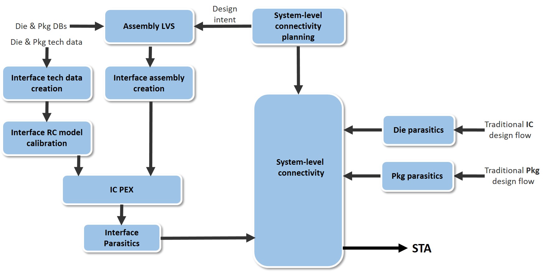
FIGURE 1. A complete HDAP parasitics flow for a digital STA process (Mentor – click to enlarge)
EDA tools
I said earlier I’d get back to the discussion of EDA tools. From an EDA perspective, building an automated flow to support these checks/analyses provides HDAP designers confidence that these processes can occur in a consistent, repeatable manner while ensuring accuracy and minimizing runtime. From a tool perspective, EDA suppliers have typically chosen one of two approaches:
- Single cockpit. EDA companies taking this path build a single simulator infrastructure to support HDAP circuit simulation and STA. Although convenient at first glance, it forces a designer to use the same design tool for all components at all levels (die and package). Although this approach would be useful when building ‘fully live’ heterogeneous HDAPs (i.e., both die and package are under simultaneous development, and can both be edited for performance), this is rarely the case. More commonly, known good dies (which have already been taped out) are used to build an HDAP. In this case, the cockpit approach may be too restrictive, given that HDAP design and verification typically require the involvement of multiple groups with varying backgrounds and tool preferences.
- Tool-agnostic. EDA companies that select this approach enable designers to assemble the required HDAP system-level connectivity (including parasitics), regardless of which design tools they use to build any one die or package. Once this system-level connectivity is available, the designer can export it in the required format to any circuit simulation/STA tool to simulate or analyze the entire HDAP. The advantage of this system for companies already in the package design business is that it introduces minimal disruption to their existing tools and methodologies.
Conclusion
As the use of HDAP designs becomes more popular, the need for post-layout simulation (analog) and post-layout STA (digital) flows to augment basic physical verification (DRC and LVS) is obvious. While tools exist that can automate much of the process of accumulating the necessary data for these analyses, an understanding of the actions being performed provides designers with confidence in the accuracy of the results. Confidence in HDAP manufacturability and performance is essential to their continued growth and market success.
References
[1] John Ferguson, Tarek Ramadan. “The Future of Package Design Verification: Assembly Design Kits.” Mentor, a Siemens Business. October, 2015. h
[2] Andy Heinig. “Why Use An Assembly Design Kit And Assembly Design Flow?,” Semiconductor Engineering. February 8, 2018.
https://semiengineering.com/why-use-an-assembly-design-kit-and-assembly-design-flow/
[3] John Ferguson, Tarek Ramadan. “Assembly Design Kits are the Future of Package Design Verification,” 3DInCites. August 3, 2015.
https://www.3dincites.com/2015/08/assembly-design-kits-are-the-future-of-package-design-verification/
[4] Tarek Ramadan. “Crossing the Chasm: Bringing SoC and Package Verification Together with Calibre 3DSTACK.” Mentor, a Siemens Business. January 2017.
[5] Tarek Ramadan. “Package designers need assembly-level LVS for HDAP verification.” Mentor, a Siemens Business. December 2017.
[6] Mentor, a Siemens Business. 2017. “Mentor extends solutions for TSMC InFO and CoWoS design flows to help customers continue IC innovations.” Sept. 13, 2017.
[7] John Ferguson, Dusan Petranovic. “Full 3D-IC parasitic extraction,” Tech Design Forum. June 8, 2014. http:// www.techdesignforums.com/practice/technique/full-3d-ic-parasitic-extraction/
About the author
Tarek Ramadan is a Technical Marketing Engineer for Calibre Design Solutions at Mentor, a Siemens Business. He supports Calibre physical verification solutions for 2.5D-IC, 3D-IC, and wafer-level packaging applications. Tarek holds BS and MS degrees in electrical engineering from Ain Shams University, Cairo, Egypt. He can be reached at tarekUNDERSCOREramadanATmentorDOTcom.