Overcoming increasing PCB complexity with automation
Advanced PCB and IC technologies have to be matched with advanced design and analysis tools if companies are going to produce board designs that are right first time, on time.
John Isaac
In a recent survey by the Aberdeen Group, (“Why PCB Design Matters to the Executive”), 53% of electronics company respondents said that increasing PCB complexity was their main challenge as they tried to get the most competitive product to market more quickly and at reduced cost. The technology advances that helped make their products more competitive had also made their designers less productive and increased overall design cycle times. The top 20% of ccompanies contacted for the survey said they used design best practices to overcome these challenges.
Complexity is Increasing Exponentially
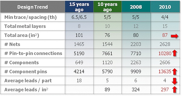
Several factors are contributing to increasing PCB complexity. Mentor Graphics has been running a Technology Leadership Awards (TLA) program for the past 23 years to recognize designers and how they overcame challenges in their design processes. By capturing statistics from the many PCBs entered into the competition over the years, we can track technology trends, as shown in Figure 1. Of particular note:
- Board area has remained relatively constant, while the number of leads per square inch has tripled in the last 10 years.
- The average number of components has quadrupled in 15 years while the average leads-per-part has decreased by a factor of 4-5x. This reflects the increasing use of a few, very high pin-count parts, combined with the passive components (such as terminating resistors and decoupling caps) that are necessary to support high performance interconnects.
- The number of pins in a design has tripled and the number of pin-to-pin connections has doubled.
Figure 1
Statistics from the Technology Leadership Awards program show clear trends in complexity. (Source: Mentor Graphics – click image to enlarge)
Performance, Heat and Manufacturability
Figure 1 illustrates a part of the complexity challenge. Significant increases in IC speeds and densities have made designing advanced PCBs more difficult in a number of other ways.
1 – The proportion of high-speed interconnects that must meet strict design rules
In several TLA entries, a very high proportion of nets had to meet strict design rules that affect performance and signal integrity. In one case, 93% of interconnects had to meet signal-integrity constraints. With the emergence of SERDES and DDRx interconnect standards, some nets now have to be kept short and meet very tight matching-length tolerances.
2 – The thermal impact of high performance
Despite attempts by IC suppliers to cut power dissipation, as IC speeds and densities increase so does the heat they dissipate. And putting these ICs into smaller and smaller form factors compounds the problem. This causes significant thermal management challenges that must be met at the IC package, PCB and system levels.
3 – The need for multiple voltage levels at tight tolerances
Several years ago, all ICs ran on +5V, so a board’s power system could run on a single voltage and ground plane. Today, ICs run at multiple supply voltages, some of which can be as low as 0.9V. A complex PCB may have to accommodate up to 30 power distribution networks (PDNs) which have to be jig-sawed into as few layers as possible. PCB designers must design these finely tuned PDNs with enough (but not too much) copper to meet DC specs and distribute enough de-coupling capacitors (but not too many, as this would raise the cost) to meet AC specs.
4 – Manufacturability issues
The use of finer tolerances, smaller components, denser BGAs and even flip-chip mounting means that PCB designers need to check their work for manufacturing violations, and apply best practices that help improve yields and increase reliability. These rule sets can be very extensive (some have grown to more than over 700 entries), putting them beyond the comprehension of the average designer to track during layout.
All is Not Lost
How can a company expect to apply advanced PCB technologies and still meet productivity and time-to-market goals? Part of the answer is to ensure that the tools they are using have kept up with the challenges of these advanced technologies. Here’s some of the capabilities required in today’s tools.
High-Density, High Pin-Count BGAs
Today’s IC packages have more pins at smaller spacing. This is great for squeezing more functionality into smaller spaces, but the problem is routing from those dense BGAs to the rest of the PCB. This is usually done in two steps. The first is to connect from the surface BGA pads into the inner layers of the PCB (the fanout). The second is to connect from those inner-layer vias to the rest of the components on the PCB. This process can take a layout designer days of interactive routing if handled manually.
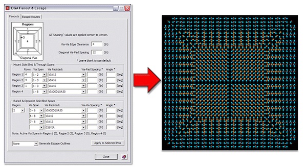
Some design tools can automate this process, developing the interconnect in minutes versus days. The first step is the fanout. This can be done using either HDI/Microvia layers or through-vias. The basic methodology is described in a recent book* by Charles Pfeil and automated in systems such as Mentor Graphics’ Expedition™ Enterprise toolset. The first step enables the user to define a fanout pattern. Figure 2 illustrates the process of using a template to define the fanout pattern. The actual fanout routing takes seconds with an automated function.
Figure 2
Example of Mentor’s automated fanout using a template and HDI/Microvias. (Source: Mentor Graphics – click image to enlarge)
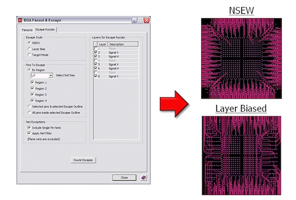
The second step is to connect from this fanout to the rest of the board. There are two ways to do this. The first is to apply a ‘North-South-East-West’ pattern, which uses the layers and escapes to the nearest edge of the BGA. The second is a ‘layer-biased’ approach in which the breakouts go in the direction of the interconnect and are biased to the layer direction. Figure 3 illustrates these options.
Figure 3
Illustrations of both the ‘North-South-East-West’ and the ‘layer-biased’ automated breakouts. (Source: Mentor Graphics – click image to enlarge)
Performance, Performance, Performance
Increases in IC density and performance have affected PCB design. The first effect is the increase in the proportion of high-speed interconnects that must be finely tuned for delay, crosstalk and signal integrity. Such PCBs need to be simulated and analyzed to ensure that the critical signal corner cases meet spec at extreme temperature and manufacturing tolerances.
Advanced design systems enable engineers to pre-analyze the high-speed net classes and set up constraints for those interconnects. These constraints are carried through the rest of the design system and available to the layout and the post-layout analysis steps. During layout, whether the CAD design is performing interactive or automatic routing, the constraints are followed to meet the length (delay), parallelism (crosstalk) and tolerance (matching) specs. For boards with many constrained interconnects, this automation provides the productivity and accuracy to produce a correct board the first time, on time.
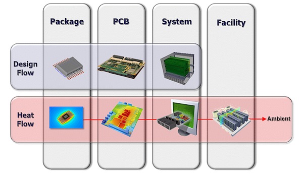
The second high-performance issue is thermal management. If the junction temperature of an IC goes above its specified level, the IC suffers both reduced performance and long-term reliability issues. Solving the heat management problem is a multi-level task (see Figure 4).
Figure 4
Thermal analysis at all levels of the product needs to be performed to manage the heat dissipation of today’s high performance systems. (Source: Mentor Graphics – click image to enlarge)
The IC package must be designed to provide adequate heat dissipation to its extremities. The PCB is affected by the placement and proximity of the hottest components. The final product’s heat dissipation capabilities are affected by systemic issues such as the enclosure, fans, heat sinks, rails, etc. There are very few tool suppliers that can provide a thermal analysis solution at all three of these levels, especially since the system-level analysis is usually performed by a mechanical engineer, with PCB design data supplied by the PCB designer plus the MCAD design of the enclosure. If it were not possible to do a thermal analysis of a virtual prototype using software such as Mentor’s FloTHERM, the other (costly, time-consuming) option is to build physical prototypes, test them and then make design changes.
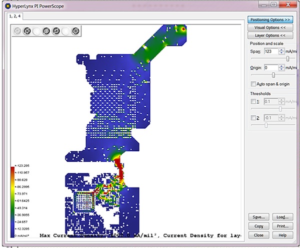
The third issue is the design of the PDNs to support the multiple, low-tolerance voltages needed by the onboard ICs. As the CAD designer is jig-sawing these complex PDN shapes into the limited PCB layers, she or he may believe that they have supplied adequate copper to support the DC requirement of voltage levels and low current densities. However, through-vias and pins (Figure 5) can reduce the effective amount of copper at bottlenecks. DC power-integrity analysis can accurately analyze the PDN and highlight potential problem areas, which can be fixed with additional copper or vias to carry the currents. Another issue with PDNs is supplying noise-free voltages to the ICs. Noise can be generated by multiple IC power pins switching at once, causing the PDN to act as a transmission line and produce varying (noisy) voltage levels. Power integrity analysis can show where to add decoupling capacitors to ensure that adequate, noise-free voltages are supplied throughout the PDN.
Figure 5
Mentor’s HyperLynx Power Integrity analysis function can analyze complex PDNs for DC and AC issues. (Source: Mentor Graphics – click image to enlarge)
Manufacturability
Design for manufacturability (DFM) means more than looking for and correcting design violations that will cause production failures. Designers must strive for high yields during board fabrication and assembly, as well as long-term product reliability. With up to 700 rules and best practices to follow, board designers need help from software to check the rules during the design process. This software is embedded in PCB layout products such as Mentor’s Expedition Enterprise, runs periodically during the layout process, and provides cross-probing to highlight DFM violations in the layout environment. This same software is often also used by the manufacturer to check the design data you deliver, which helps ensure a ‘correct first time’ and highly manufacturable product ready for volume production.
Overcoming Complexity with Automation
The downstream effects of applying PCB and IC technology advances is the risk of compromising the electronic company’s time-to-market and design team productivity. Fortunately some PCB design tool suppliers have kept up with these advances and can provide the automation necessary to keep designers productive and produce competitive products, on time and at the lowest costs.
*Pfeil, Charles, BGA Breakouts and Routing, LL Publishing, 2008.
John Isaac is Director of Market Development for Mentor Graphics’ Systems Design Division. John has worked in the electronic design automation industry with PCB and IC technology for more than 40 years. John has held marketing positions in both PCB and IC product areas at Mentor Graphics. He is currently responsible for worldwide market development for the Systems Design Division.
