Part 3 – A unified, scalable SystemVerilog approach to chip and subsystem verification
The article describes LSI’s work on the use of a single SystemVerilog-based (SV) verification environment for both the chip and its submodules. The environment is based on SV’s Advanced Verification Methodology (AVM) libraries, although alternatives are available. One particular reason for choosing AVM was that LSI wanted to leverage its transaction-level modeling capabilities as well as other “advantages.”
“A verification environment that offers reusability, scalability and automation allows our verification experts to focus on the functional verification goals of a complex SoC much more efficiently,” says Thomas Kling, engineering manager for Custom SoC Products in LSI’s Storage Peripheral Division.
The main part of the article describes the environment’s development and application to a specific design: a multi-million-gate storage controller ASIC equipped with a variety of interface standards and intellectual property blocks, and expressed at the RTL in multiple languages. “In using the described approach we were able to increase our engineering efficiency and maintain a high level of flexibility for reaching our verification goals on time,” says Kling.
The ability to perform chip and submodule verification within a unified and scalable SystemVerilog (SV) environment minimizes the effort required for testbench development and frees up resources for work on the primary test cases specified in the verification plan.
The right combination of SV verification libraries (as found in the Advanced Verification Methodology (AVM) and the Open Verification Methodology (OVM)), SV Assertions and integrated processor models covers all verification needs. It offers the wide range of configurations needed to ultimately achieve dedicated submodule verification at maximum simulation speed without simulation overhead.
This approach reduces the overall time needed for functional verification of a system-on-chip (SoC) and its corresponding submodules by exploiting several inherent advantages. These include scalability, automation, flexibility and reuse.
- The test environment is configurable at a high level, so the user can focus tightly on the part of a design that must be verified. Both top module and submodule verification tests can be executed.
- Automation includes test and data generation, self-checking tests and regression mechanisms.
- The user can employ multiple stimulus techniques—these can include direct stimulation for integration testing, randomized stimulation for higher levels of abstraction during block-level testing, and processor models.
- Finally, the environment can be established as an open framework. The transactor models and scoreboards include standardized transaction-level modeling (TLM) interfaces. This greatly reduces ramp-up time for the verification of new designs.
Traditional verification methodologies use separate environments for chip and submodule verification. By contrast, the newer, more integrated strategy described here provides improvements in efficiency that more than repay the extra effort required during the initial set-up and to manage the increased complexity of the resulting environment. Moreover, only one environment now needs to be developed to cover all top-level and submodule verification tasks, and the increased complexity can be resolved by a well-defined class, directory structure and documentation.
The paper describes the SoC verification process for a specific chip to illustrate the approach. The design was a state-of-the-art, multi-million-gate storage controller ASIC including a variety of interface standards, mixed-language RTL and intellectual property (IP) blocks. The top-level module was captured in VHDL. It contained VHDL, Verilog and SystemVerilog RTL components, with multiple IP blocks as both hard and soft macros (Figure 1). The SoC could be partitioned into three main parts: an ARM subsystem with three CPUs, a host subsystem containing the host interfaces, and a subsystem with customer logic.
The environment
The SV environment was built on top of an AVM library to take advantage of the methodology’s TLM features. You can also use OVM or other libraries. Several transactors served the different external interfaces (e.g., SAS, SATA, Ethernet and various memory interfaces). We used SV’s ‘interface’ construct so that tests could access the device-under-test’s (DUT’s) internal and external interfaces. All transactors outside the SV environment (e.g., memory models, ARM trace ports) were instantiated in the top-level testbench along with the DUT and the SV verification environment.
Source: LSI
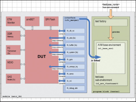
FIGURE 1 Testbench structure.
The SV environment itself was instantiated inside a program block in the top-level testbench file. This gave us the option of using ‘force’ instructions in tests where considered necessary. We also used a test factory class that generated a user-selectable environment object during runtime. To achieve this, the simulator call included a parameter that selected the type of environment class to be used as the test environment. This allowed us to construct different transactor configurations in each test. It also allowed us to run different tests without recompiling and restarting the simulator: when one test was finished, the corresponding environment object would be destroyed and the next test’s environment object was constructed and started.
The environment consisted of a base class that included all objects common to each test as well as the three AHB drivers. All tests were derived classes from this base environment class formed after individual selection of additional testbench modules (e.g., scoreboards, reference models, monitors and drivers for the DUT’s internal interfaces).
Test strategy
This primarily took two approaches to verification. Many tests covered control functions that were verified by applying directed tests, often supported by assertions to get feedback on the functional coverage. When it came to data path testing, we used a more suitable directed random approach. These tests were appropriate for testing the memory paths, Ethernet packet transfers, and SAS and SATA frame handling.
So, for the directed random approach, we implemented memory-based, self-checking capabilities. Data accesses were randomly applied to both the path-to-be-tested and a virtual reference memory model. All the read data packets were then routed to a scoreboard for comparison.
We made heavy use of assertions to make sure we covered all possible access modes on the buses and all functional capabilities of the relevant submodules (e.g., bridges). All test classes were completely self-checking and a detailed test report was provided after every simulation run.
Structure
Our testbench’s top level was a SV module with different functional sections. In its first section, we defined the SV interfaces and necessary code to instantiate and connect the DUT. A section with conditional instantiations of simulation models followed. Depending on ‘define’ macros inside the starting script, we could attach several different models at the DUT’s boundaries (e.g., Fibre Channel transceivers, SAS and SATA models, DDR & flash memory models, and ARM boundary scan trickboxes (BSTs) & embedded trace macrocell (ETM) models).
The next section included different groups of proprietary connections and several blocks of SV ‘bind’ instructions. All these were separated by their functionality into ‘include’ files and again included, depending on the ‘defines’. These blocks were used to connect empty wrapper ports inside the DUT to SV interface signals, and the ‘bind’ blocks brought additional assertion checker modules into the RTL design. The final section contained the definition of a program block (outside the testbench module) that oversaw the construction and control of the test environment and its instantiation.
As shown in Figure 2, the environment base class (‘cl_env_base’) had all the internal drivers instantiated and connected to local virtual interfaces. Only the AI-1B drivers were left to be inserted on demand in a derived testcase class. As most of the drivers handled accesses to memory-mapped regions, they were connected to ‘Memory Slave’ units that simulated memory arrays of customizable size.
If we had used configurations in which real RTL was used instead of the empty wrappers, the affected drivers’ interface connections would simply be left unconnected. But as all were used in most testcases, they were implemented in the base class.
As some tests involved using AI-1B bus functional models (BFMs) while others used ARM design simulation models (DSMs), we decided to instantiate the AI-1B transactors inside the testcase-specific classes. These were derived from the base class and, therefore, inherited all the base class’s transactors and connections.
In each testcase class, we could define the specific AI-1B transactor to be used (or none where we used DSMs), as well as all the test-supporting infrastructural models (e.g., scoreboards, stimulus generators and reference models). The testcase class also contained the actual test inside the ‘run ()’ task. The general control flow of all involved models was implemented here.
Through the SV interfaces and their connection to the environment, it was now very easy to build a largely customizable periphery around the DUT. Most test-specific transactors were defined inside the environment; only the static ones were directly instantiated at the top level. Even there we could customize the transactors using different ‘define’ parameters.
Given also the option to replace RTL parts of the DUT (or even whole subsystems) with empty wrappers connected by SV interfaces to dedicated transactors in the environment, we could now use one environment to test blocks or subsystems of the design as well as the whole chip.
For example, we had some tests that verified only the Ethernet interface and the attached frame buffer memory, while other tests verified the different ARM subsystems on a stand-alone basis. Of course, we finally used the complete DUT design for chip-level verification.
The AVM-based approach also allowed us to integrate large customer-designed parts that were provided late in the project schedule. We simply inserted empty wrappers, connected them to our transactors, and verified the interfaces to the customer logic. Later we replaced the wrappers with the real RTL, dynamically removed the transactors, and were able to reuse all the available tests.
Connectivity
In the top-level testbench we defined SV interfaces and assigned DUT ports to their signals (Figure 1). For the internal connections to the empty wrapper modules in the design, we connected the wrapper’s ports to the corresponding SV interfaces. Inside the environment base class, we had a virtual interface defined for each interface used in the top level. Both interfaces and virtual interfaces were connected at simulation start-up time to provide signal access to the environment.
Source: LSI
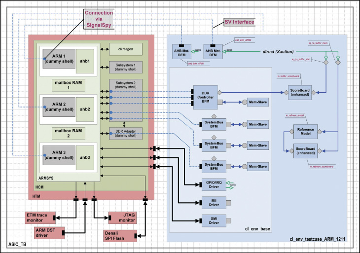
FIGURE 2 Verification environment.
To make life a little easier, we defined an additional ‘merger’ interface that had all the other interfaces nested inside, so we only needed to route one interface through the environment hierarchy instead of a dozen.
When a wrapper was later replaced by real RTL, the ‘include’ file that built the connections was not included, resulting in an unconnected interface. On the other side, we would not generate the corresponding driver anymore, thus maintaining a fully working environment.
For some tests, especially DSM-related ones executed on an ARM CPU model, it is worth having a transactor connected to an internal interface even when the RTL code is used. We had some transactors that established a communication channel (through accesses to dedicated memory areas) between the C program running on an ARM DSM model and the SV testbench routine.
For this to work we had to leave the ‘include’ files integrated after replacing the wrappers with RTL, effectively connecting the SV interface signals to the real RTL module’s ports. Another helpful technique was to add an SV interface for debugging purposes to the merger. As signals inside a SV interface can be displayed in a waveform (unlike SV dynamic variables or objects), we could assign values to such ‘debug interface’ signals inside an SV transactor to watch them in the waveforms. This took away a lot of pain during the SV transactor development and debugging process.
Verification components
The most difficult task was the integration of all the required transactors, especially the provision of a simple and unified access method for the test writers. To illustrate: we had to use some drivers (e.g., SAS/SATA) that were available only in Verilog; our Al-TB driver was a reused and quite complex module written in pure SystemVerilog; and we needed to code several new transactor classes.
We developed new drivers for several different internal bus protocols as well as a basic Ethernet driver, memory transactors, enhanced scoreboards capable of comparing out-of-order transactions, reference models and testbench-supporting transactors. These transactors enabled synchronization by event triggering and message passing between the SV environment and C routines running on the DUT’s ARM subsystems.
As our goal was to take maximum advantage of the TLM features to simplify the interconnections between the transactors and unify their utilization, we put some effort into making as many components AVM-compliant as possible. This was also very important with regard to plans for our subsequent reuse strategy and later migration to the OVM library for future projects.
Using the AVM library saved resources that were no longer taken up in handling the details of managing transaction movement inside an environment. The predefined TLM structure made it possible for a single engineer to plan, build and maintain the whole environment, including most of the transactors. The rest of the team could concentrate on RTL development and test writing.
Converting the Fibre Channel and SAS/SATA Verilog transactors to SystemVerilog and AVM was not feasible within this project’s schedule, but these tasks will be undertaken for our next-generation environment. Porting our already available SV Al-TB driver to AVM compliance required some changes in its internal structure, but was accomplished in a reasonable time. The development of all the new transactors was accomplished ahead of schedule thanks to the easy-to-use structural TLM building blocks of the AVM library.
LSI
Orleansstrasse 4
81669 Munich
Germany
T: + 49 (0) 89 45833 0
W: www.lsi.com