DVFS and body bias
Dynamic voltage and frequency scaling (DVFS) is a technique that takes advantage of the quadratic relationship between supply voltage and circuit power consumption to improve overall energy usage, making it a candidate for low-power VLSI design. There are tradeoffs to be made. Because circuits operating at a lower voltage will generally run more slowly, frequency of operation often needs to be scaled as the voltage reduces.
Although the equation for switching power in CMOS circuits P = k.CfV2 suggests that reducing voltage as far as possible will minimize energy – pointing to operation close to or below the threshold voltage (Subthreshold Guide) – the effect of leakage needs to be taken into account. In nanometer processes, the effects of leakage are severe and can easily exceed the benefits of cutting switching power through voltage and frequency reductions – resulting in higher energy overall even though the instantaneous power demand will generally be lower.
The effects of leakage have made DVFS less attractive as a power-management and energy-reduction strategy in leading-edge processes than for older technologies that can offer better leakage control. A common alternative strategy is to run the circuit at full speed but use power gating to cut the supply when it has completed.
However, the possibility to use dynamic body-bias techniques in FD-SOI and potentially future finFET processes has rekindled interest in the DVFS. Using reverse body bias it is possible to cut leakage while the circuitry is expected to run slowly. Forward body bias can provide a speed boost for circuits, allowing them to complete a task quickly and then use power gating to avoid incurring a leakage penalty when not operating.
Applying DVFS
In order to apply dynamic voltage scaling, designers need to analyze how the system is managed dynamically and then find good control policies, which could be predictive, adaptive or a combination of both. The IC needs to be divided into domains that can be supplied with different clock signals and voltage levels. Control software and hardware are used to ensure each domain gets the right combination of voltage and clock signals. As with voltage islands, level shifters and synchronizers are needed to ensure that logic levels are adjusted correctly as the signals cross from one domain to another.
The use of DVFS across multiple regions on an IC may push designers towards the use of a globally asynchronous, locally synchronous (GALS) design style (GALS Guide). This style treats logic within each clock domain as synchronous but communications between blocks are handled asynchronously using handshake protocols.
Body bias provides further control
In conventional CMOS design, the body of the transistor stays close to 0V. The voltage on the gate electrode provides the potential difference needed to switch the device on and off. Altering the voltage of the silicon body relative to the gate can help activate the transistor using a lower gate voltage. Alternatively, the use of a reverse body bias will push that activating voltage higher. This has the effect of reducing subthreshold leakage.
Reverse body or back bias can temporarily cut the power consumption of inactive transistors without involving complex logic in the decision to power gate a circuit and save register state. This allows quiescent circuits to move back into the active state much more quickly than those that have been power-gated.
Because of parasitic effects, advanced bulk-CMOS processes are limited in the degree to which they can apply body biasing, typically to within several hundred millivolts. FD-SOI offers a greater opportunity for forward and reverse body bias, an option that is not currently available to finFET processes although work disclosed at the 2014 VLSI Technology Symposium indicated that mechanisms for implementing body bias.
A 28nm FD-SOI test chip by STMicroelectronics that incorporated the ARM Cortex-A57 used forward body bias to increase the peak frequency to 3GHz at the full supply frequency. By operating at a nominal 0.5V, the circuitry ran at a much slower 300MHz but with reduced power consumption.
Similarly, at the 2014 International Solid State Circuits Conference (ISSCC), research institute CEA-Leti and STMicroelectronics described a DSP that cut the operating voltage to 400mV with the assistance of forward body bias to support a clock speed of more than 450MHz. Clock speed increased to 2.6GHz with a nominal supply voltage of 1.3V, an estimated doubling in performance compared to a non-biased architecture.
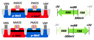
Image Conventional-well (top) and flip-well (lower) structures for back bias on FD-SOI (Source:ST)
FD-SOI does not provide the designer with complete freedom over the bias direction. The conventional well structure – doped in the opposite manner to the drain and source – allows for up to 3V of reverse bias. To provide up to 3V of forward bias and effectively overdrive the transistor, CEA-Leti and ST developed the ‘flip well’ structure, that swaps the normal doping for its opposite – the NMOS transistor is placed in an n-doped well and the PMOS in its p-doped counterpart. The transistor can be biased in the opposite direction but only up to -300mV, similar to a bulk process. The standard well structure cuts leakage approximately six-fold through reverse biasing, with just 300mV available for a small performance increase.
Through process modification, startup SuVolta is trying to bring greater control over body bias to bulk CMOS processes. The SuVolta technology adds buffer layers underneath an undoped silicon channel, with body biasing available to control performance. Fujitsu launched an image processor in 2013 using the technique to achieve a claimed 30 per cent power reduction compared to existing products.


