Choosing a block representation in a UPF-based hierarchical multi-voltage IC design
This article looks at the way in which various representations of a block of a design have different implications in a UPF based power-aware hierarchical design flow.
As a design grows, so do the implementation challenges. A large design may be subject to more physical effects, be more vulnerable to process variation, and have more operating scenarios than a small design. This may require analysis at many design corners, leading to a trade-off between overall accuracy and tool runtime.
Hierarchical design
How can a large design be implemented in a reasonable turnaround time (TAT) and meet its performance, power and area (PPA) requirements? Standards such as UPF help express the designer’s power management intent throughout the elaboration of the design. In terms of actually doing the design, there are two basic approaches.
In a flat implementation, in which designers produce full-chip RTL, the design flow is simpler and the approach works well if TAT and machine resources are not an issue.
A hierarchical implementation, on the other hand, enables a divide-and-conquer strategy in which a team implements each block individually. This approach may reduce TAT by enabling blocks to be developed in parallel. The hierarchical approach should also make it easier to include IP. And when all the finished blocks are integrated to create the full chip, the fact that they have been modeled at various levels during their implementation means that these abstractions can be used to minimize the memory footprint of the full design.
How can we take advantage of a hierarchical flow to create a large, power-aware design? Working block-by-block from the bottom of the design hierarchy upwards, there are two ways to move forward.
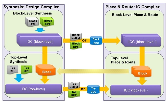
Figure 1 A hierarchical UPF implementation flow (Source: Synopsys)
In the first approach, the RTL for each block is run through Design Compiler to create a synthesized netlist of the block. This can then be married up with the top-level RTL, which defines how the blocks should be interconnected, in another Design Compiler run to create a full-chip netlist.
At the same time, each block netlist can be run through place and route in IC Compiler, with the resultant blocks being integrated with the top-level netlist in a top-level place-and-route run.
In the second approach, each block is synthesized to a netlist and goes through place and route as a block, as before. In this case, though, the data about the placed and routed blocks is fed back to Design Compiler to be synthesized into the final design alongside the top-level RTL.
Choosing a block representation
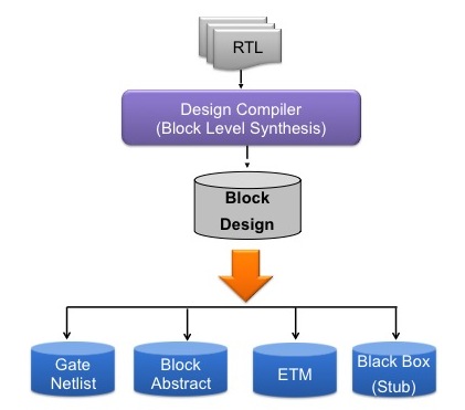
Each of these approaches involves multiple data hand-offs between tools at different stages of the flow. Design Compiler can represent the results of a synthesis in four ways: as a gate netlist; a block abstract; an extracted timing model (ETM); or a black box. The design requirements of the full chip will drive the choice of block representation for the top-level synthesis in a hierarchical implementation flow.
Figure 2 Four ways in which Design Compiler can output a design (Source: Synopsys)
The gate-level netlist is the fullest description of the block.
A Block Abstract is a structural model, based on the gate-level netlist. The block abstract captures both the I/Os and the internal logic netlist, which makes it possible to analyze paths through internal registers, and optimize the interface logic within the abstracted block, bringing greater design freedom.
An Extracted Timing Model (ETM) represents the whole design in a Liberty .lib file format. All timing paths from input to output are represented as static timing arcs. All the internal logic is hidden, and the ETM’s use of the Liberty format makes it easier to represent third-party IP. Handling the whole design as a .lib file will also reduce its memory footprint.
ETMs are generated by PrimeTime. Each design corner and mode that has to be verified will need a separate ETM, although they can be compressed into a single model.
A Black Box (or Stub) representation of a design doesn’t have any logic or timing information, which makes it small. It can also be useful way to represent the top level of a design before any block RTL is available.
Hierarchical design implementation
How would each of these models be used in a hierarchical design implementation flow?
Using Block Abstracts
A single Block Abstract file captures all of a block’s design detail, as well as the interface logic. The block-level interface logic is accessible for optimization during top-level synthesis (for example, resizing), which helps to speed up top-level design closure.
How is a Block Abstract created? During synthesis, a design is read in, any related UPF file is loaded, constraints are applied, and synthesis is run, using the
create_block_abstraction
command after block-level synthesis and before writing out the file, which will then include the full design and the Design Compiler block abstract. Hence:
create_block_abstraction
write_file -hierarchy -format ddc \
-output design.ddc
How can designers take advantage of the fact that Block Abstracts include enough of the design detail to enable the interface logic to be optimized during top-level synthesis?
Design Compiler can be told to optimize the size of block-level interface I/O cells during top-level synthesis, so that the top- and block-level interfaces can be optimized at once. IC Compiler can go further, during its route_opt and focal_opt stages, adjusting buffer sizes and placement.
Figure 3 An ETM includes enough detail to enable interfaces to be optimized (Source: Synopsys)
How is this achieved in practice? Design Compiler is supplied with the top-level RTL and floorplan, the top SDC and UPF files, and the Block Abstract, as the raw material for a synthesis run to produce an interface-optimized top-level netlist in a .ddc file. Hence:
set_top_implementation_options -block_references \
{Block1 Block2} -optimize_block_interface true
# Read in top-level RTL
# Read in blocks as block abstracts
read_ddc {Block1.ddc Block2.ddc}
current_design top
link
report_top_implementation_options
…
# Continue with top-level compile flow
Using Extracted Timing Models
If a block is represented as an ETM, a library representation of the whole design in the Liberty format, it will be treated as a leaf cell during design integration.
Using a Block Abstract model, a block-level design will be seen as a hierarchical level during top-level integration. With the ETM and Black Box approaches, the design is compressed until it looks like a leaf cell.
A UPF scope can be set on a leaf-level cell as long as it is an ETM or Black Box, and not a regular standard cell.
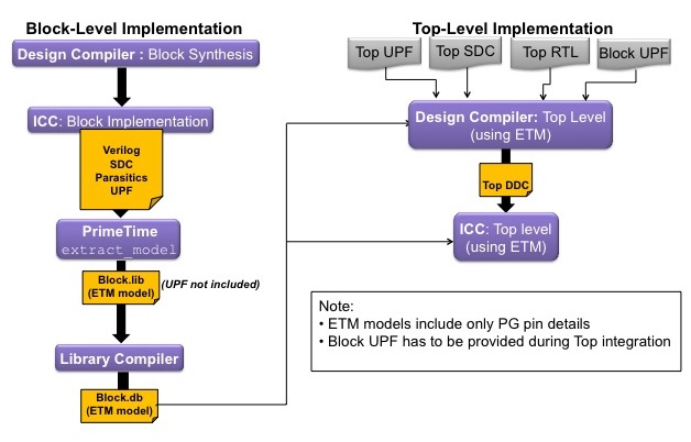
Figure 4 A hierarchical design flow using ETMs (Source: Synopsys)
How would designers use ETMs in hierarchical design? The first step is to define a block at RTL and run it through synthesis and block place and route. The output of this is a fully implemented design described in a Verilog netlist, SDC, UPF and parasitic files. These are used as an input to PrimeTime, which is run with the command extract_model to create a Liberty version of the design (as a block.lib). The block file is then used as an input to the top-level synthesis process, alongside the top-level and block-level UPFs, SDC and RTL files. The output of the synthesis is a top-level model, which is used, along with the block ETM file, as an input to top-level place and route.
Using Black Boxes
Designing with Black Boxes leaves little scope for work at the block level, other than defining what the blocks should be. To do a top-level synthesis using Black Boxes, designers must define the boundary constraints for the Black Box in a UPF file for subsequent analysis and optimization processes.
Any logic at the top level that is driving, or is driven by, a Black Box port cannot see a real driver of the load since the internal logic is, as yet, undefined. Designers must set up related supplies for the Black Box ports to enable a proper top-level, UPF-driven implementation.
If the ports do not have any related supply constraints, the tools will assume the domain’s primary supply as the Black Box’s related supply.
Using a supply_net based UPF strategy, the command:
set_related_supply_net
will indicate the related supply net of the block port.
If you are using a supply_set based UPF strategy, the commands:
set_port_attributes
-driver_supply_set |
-receiver_supply_set
are supported with supply sets.
Having set the boundary condition properly, provide Design Compiler with the Black Box block design, its related UPF file defining its boundary constraints, and the usual top-level RTL, SDC and UPF files.
Using a Gate Level Netlist
Design Compiler creates a gate-level block netlist based on the input block RTL, SDC, floor plan and UPF file. The block netlist and UPF file are then used as inputs, along with the top-level RTL, SDC, flooplan and UPF files, to Design Compiler to create the top-level file.
In the second part of this feature on hierarchical implementation strategies for multi-voltage gigascale designs using UPF, we will look at some of the associated tasks. These include:
- UPF propagation in IC Compiler
- power domain merging
- controlling power supply availability
- managing level shifter insertion
- managing Source | Sink
- managing isolation at the parent location
- isolating heterogeneous nets
Supporting materials
This article is the first of two based on a Synopsys webinar entitled A Hierarchical, Low Power Design Approach for Gigascale Designs. A second article focuses on managing power intent, signal isolation and level shifting in a UPF-based multi-voltage IC design.
Guide to UPF
Guide to IEEE 1801-2013 (UPF 2.1)
Synopsys Subset Support for IEEE 1801 (Solvnet ID: 021264)
Design Vision GUI: Low Power Design Made Easy: Create, Visualize and Debug Your Power Intent
Author
Viswanath K Ramanathan is a product engineer for Power Compiler, specializing in low power design implementation. Ramanathan has over 10 years of experience working in ASIC design, including areas such as Library characterization, logic synthesis through RC extraction, signal integrity analysis and timing sign-off. Ramanathan has a MSEE degree from Arizona State University.


