A review of model development for 10nm lithography
John Sturtevant looks at ongoing preparations for the incoming node and charts significant progress that has already been made.
The development of new manufacturing nodes is always full of adventure and discovery. While we usually see the challenges of a new node looming on the horizon like a storm at sea, it is not until active development is well underway that we get a good look at the waters. Right now for 10nm lithography – we are still looking into the storm, although it’s getting closer. The good news is that we are discovering ways that will help us chart a safe passage. As you might expect, 14nm is the pathfinder but we are developing strategies for the process beyond in its own right.
Starting with the guidance we have from 14nm research, we know that models based on a single plane will not be enough on that process or 10nm. We will need three-dimensional models to predict patterned dimensions and pattern failure modes accurately. Several innovations are helping us to navigate the associated challenges. Our main efforts target the accurate and fast simulation of 3D phenomena associated with the mask, the wafer and the resist. Let’s consider some examples.
The path from 14nm to 10nm lithography
The 3D electromagnetic field (EMF) effects associated with mask topography are becoming quite a challenge. They have been effectively modeled for many years, but at 14nm we are already refining the models for edge-to-edge crosstalk signals in domain decomposition methods (DDM). This results in significantly better matching to rigorous simulation with very little impact on runtime. We have consistently observed better wafer fitness when using the enhanced crosstalk DDM library, especially when the mask stack slope has been optimized in conjunction with the mask bias. You can go deeper into our work on EMF effects by reading this paper recently presented at SPIE Advanced Lithography.
A significant optical proximity correction (OPC) challenge has arisen at 14nm in what were formerly considered non-critical implant layers. In addition to the traditional proximity effects associated with the implant layer mask, we have found that the underlying active and gate layers can interact through a variety of mechanisms to influence the edge placement of the developed implant layer. These mechanisms include:
- bulk reflectivity differences;
- resist thickness thin-film interference effects;
- reflective notching from pattern sidewalls;
- reflections from curved surfaces; and
- focus differences.
Indeed, there are several others, and you can read more about these issues in another paper we have recently published. To capture the complex array of potential wafer effects, we have developed underlayer topography models for 14nm. These models are being expanded to better represent the impact of active finFETs and we have already seen excellent results for pre- and post-poly layer implant models.
A third 3D challenge concerns the photoresist model. The 14 and 10nm nodes use negative-tone develop (NTD) resist processes extensively for the patterning of the metal and via layers, exploiting the intrinsic aerial image advantage of a bright field mask. These NTD resist processes have unique shrinkage and develop rate properties compared to the traditional positive-tone processes, so we have updated the compact model (CM1) to support new NTD-specific model forms. These forms consistently show a 25-30% improvement in accuracy for the prediction of wafer results. Improvements in the prediction of resist toploss and scumming – as well as SRAF printing for both PTD and NTD cases – have been achieved over the past year.
Faster models for 10nm lithography
Accuracy is not the only consideration. Time is also important – in this case, the time it takes to obtain and verify a model. Viable 10nm lithography will require full-chip capable models for 50 or more layers, and these models will frequently have to be redone as processes evolve. Today, calibration can last several weeks. It is taken up by test pattern selection, metrology tool recipe setup, wafer measurements, data filtering, and finally model calibration and validation. As shown in Figure 1, the target is a 50% reduction in the cycle time.
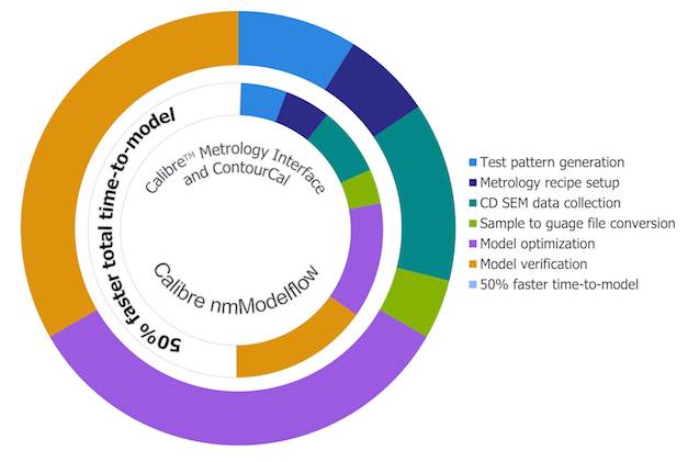
FIGURE 1. Toward a 50% reduction in modeling cycle time for 10nm lithography (Mentor Graphics)
In context, what we are seeing here is a contrast between current and proposed strategies. Model development typically takes 5-15 days for test pattern generation, metrology recipe setup, and CD SEM data collection, and another 12-30 days for model optimization and verification. Advanced model flow software can reduce total time-to-model by 7- 20 days for 10nm lithography.
Several software technologies can help in this regard. One example is an interface that enables offline generation of Applied Materials or Hitachi CD-SEM recipes based upon GDS data. This can take hours and in some cases days off the flow.
Another time-saving technique uses the entire shoreline extracted from CD SEM contours to generate many more data points than are typically obtained with ‘gauge-based’ single CD inputs –the typical increase in the number of data points here is of several orders of magnitude. Since the full SEM image is available, far fewer image collections have to be undertaken for contour-based modeling. So, the metrology setup and execution time can be cut dramatically. Customers who have already used this technique have seen a 5X cycle time improvement in addition to better model accuracy than for an all-gauge case.
Finally, we need to mention an innovative model calibration platform that features a new architecture for parallelization, new optimization routines, a new database, and an improved GUI. It should deliver at least a 3X improvement in the time-to-model for 10nm lithography.
Model calibration flows have typically employed fewer than 16 CPUs to optimize the degrees of freedom associated with the mask, optics, resist, and etch models. Also, these models have been tuned in a serial fashion. The new platform scales to more than 1,000 cores, which offers the potential for dramatically faster model calibration. This is especially true for the platform’s ‘joint calibration mode’ where mask, optics, and resist parameters are concurrently tuned. Such an approach is shown to yield up to 17% more accurate final models.
The cycle time reductions and greater accuracy of the new technologies discussed here will be a key enabler for OPC teams in the coming years. Drawing on new models and advanced new modeling calibration tools, I think we will weather the waters of 10nm lithography development with some confidence.
Further reading on 10nm lithography
Rapid, accurate improvement in 3D mask representation via input geometry optimization and crosstalk
Full-chip correction of implant layer accounting for underlying topography
About the author
John Sturtevant is the director of Modeling and Verification Solutions at Mentor Graphics.

I need to develop the accurate RC delay model for Tri Gate FinFET. Can you please help me.