Give the people what they want: toward making 3D IC mainstream
The semiconductor industry faces an inflection point. Higher cost, lower yield, and reticle size limitations are driving the need for viable alternatives to monolithic solutions. Those traditional solutions are hitting or coming close to the limits of manufacturing and physics. This is driving an emerging trend to disaggregate what typically would be implemented as an SoC into solid, fabricated IP blocks, otherwise known as chiplets.
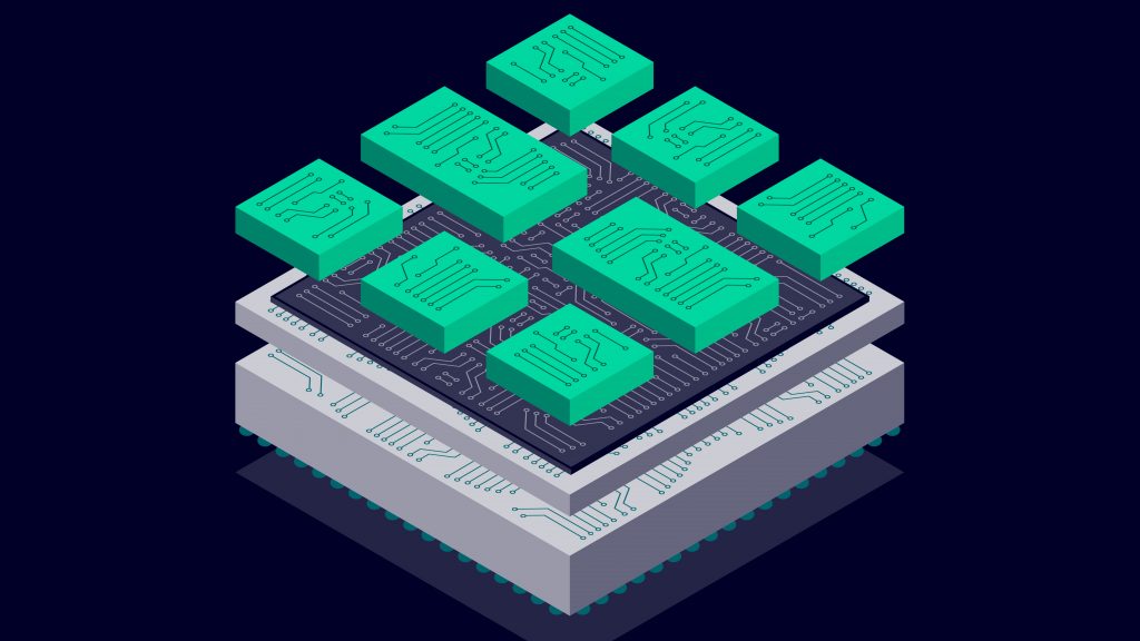
Chiplets typically provide a specific function implemented in an optimal chip process node. Several chiplets and an optional, custom SoC device can be mounted and interconnected in a single package using high speed/bandwidth chiplet-to- chiplet interfaces (Figure 1). The resulting 3D IC heterogeneously integrated packages deliver greater performance at a reduced cost, higher yield, and have only a slightly larger area than a traditional monolithic SoC package.
But all these benefits and advantages come at the price of adopting an advanced and sophisticated technology. In this case, the level of interactions, requirements, and signoff approvals increases, bringing new demands and challenges.
Our goal is to approach the adoption of 3D IC packages through a stepwise linear process. This allows mainstream companies, as well as the big players, to progress smoothly and successfully from where we are today into this next-generation design environment.
To that end, this article outlines five workflow adoption focus areas that provide immediate heterogeneous integration capability benefits while establishing a managed, methodology adoption and migration process that minimizes disruption, risk, and cost. These five workflows bring heterogeneous integration-based chiplet design within reach of the mainstream instead of only the largest IDMs and fabless semiconductor companies.
These five 3D IC workflows span several interlinked domain areas:
- Architectural definition is enabled by chiplet design kits (CDKs) that provide a model of the chiplet for implementation and integration. A CDK can include interface protocols, IO models, ATE test methods, power characteristics, and thermal models such as BCI-ROM.
- Design activities then include planning, prototyping, system technology co-optimization, and detailed physical implementation of the substrates. Heterogeneous planning and co-optimization should use a complete 3D digital model (aka digital twin) of the entire device assembly that drives all downstream aspects of design, analysis, and verification maintains a continuous digital thread.
- Multi-physics analysis deploys physical verification at every level of 3D assembly, from the substrate layer through design rule checks to assembly-level layout-versus-schematic.
- Device-level test targets multi-domain testing starting with the individual die and continuing with die-to-die and across the entire package assembly.
- Manufacturing is informed by ecosystem interoperability, that includes the ability to seamlessly share designs and data with suppliers, partners, foundries, and OSATs.
For a broader discussion on the factors driving the chiplet design revolution and the new challenges they present, and for an in-depth explanation of the five workflows that address and manage them, please read the full paper Five key workflows that deliver 3D IC packaging success.
 Keith Felton is product marketing manager for High Density Advanced Packaging at Siemens EDA.


