Accelerated VIP solves firmware and driver integration and validation tradeoffs
Trying to balance your use of simulation and FPGA prototyping is tough. Acceleration used with Accelerated VIP offers simulation-like visibility and debug with near FPGA performance.
Today’s SoCs include a large (and growing) amount of software. Typically, the base platform that underlies user applications includes an operating system (OS), drivers, firmware, diagnostics, and test software. Much of that platform is embedded or ‘bare metal’ software that interacts directly with the hardware. Integrating and validating embedded firmware and drivers requires that the software be validated in conjunction with the RTL. As such, virtual platforms or processor emulators, which are used commonly to validate user applications, are insufficient.
Because of the RTL interaction requirement, firmware/driver developers have traditionally been forced to make a painful tradeoff decision between using a simulated environment with an FPGA prototype or having to wait until actual silicon is available. This article discusses those tradeoffs and introduces a strategy that provides the best of both simulation and FPGA prototypes: The use of acceleration and Accelerated Verification IP (AVIP) for firmware integration.
The tradeoffs between simulation and FPGA prototypes?
RTL Simulation provides high accuracy and good-to-excellent hardware debug capability. But it runs slowly. It is possible to use transaction-level model (TLM – Guide) simulations which run much faster than RTL simulation but which sacrifice on hardware accuracy and timing.
That’s why users often prefer the alternative: an FPGA-based prototype. These run fast but you must wait until a prototype is constructed (or, even longer sometimes, until silicon is back from fabrication). In other words, FPGA prototypes are delivered late in the cycle. And, when they finally arrive, they offer limited hardware visibility and debug capability.
Fortunately, the need to make that tradeoff decision is being obviated with simulation acceleration platforms together with AVIP. Acceleration with AVIP provides the best of both worlds: It delivers high performance, is available early in the verification cycle, and provides excellent debug capability.
AVIP allows engineers to achieve speeds that are tens-to-hundreds of times faster than with simulation. Well architected AVIP minimizes the time spent on the accelerator. And since users must perform a variety of verification tasks during the life of the project, Cadence Design Systems has developed AVIP that provides a selection of user interfaces, each optimized for a specific task. This also delivers control over the tradeoff between performance and verification functionality (such as checking and coverage).
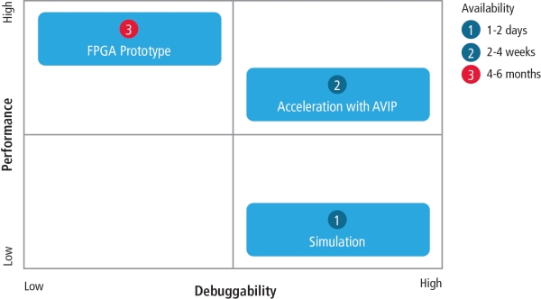
Figure 1 is a graphical depiction of each alternative’s strengths and weaknesses.
Figure 1
Comparison of alternatives for software integration and validation (Source: Cadence Design Systems – click image to enlarge)
Common software integration and validation challenges
Software integrators face a variety of challenges. These include host driver development and debug, firmware integration, and peripheral controller validation including end-to end direct memory access (DMA) transfers.
In an SoC the dedicated hardware will always be faster than the processor, and much faster than actual software execution. As a result, the system must have a robust handshake between hardware and software. It cannot rely on the timing of software running on the embedded processor to work properly. Therefore the main tasks facing software developers include:
- configuring the device properly;
- passing data properly to/from higher layers of software; and
- interrupt handling, particularly in the context of other task that the system is doing.
These requirements for software/firmware/driver validation drive a need for strong, combined software and hardware debug capability. This generally includes the needs to view the code, set breakpoints, perform single stepping, and view register and variable contents. This requires a software development environment. As one example, Cadence’s Palladium XP Verification Computing Platform, a key part of Cadence’s System Development Suite, provides integrated software debug capability. In addition, Cadence supports ARM’s popular Development Studio and RealView debugging tools.
The effort will often include validating end-to-end DMA transfers. Since it is common for these transfers to move large amounts of data, this validation can consume a great deal of time in simulation. The acceleration environment addresses this challenge effectively. There are typically two main areas of interest for a DMA transfer: (1) Does it start properly? (2) Does it finish properly? Dramatically speeding up the run time with acceleration enables engineers to quickly validate both conditions.
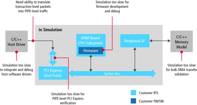
Figure 2
Common software and SoC validation challenges addressed by acceleration (Source: Cadence Design Systems – click image to enlarge)
Acceleration for firmware/driver integration and validation
The need for speed grows more pressing with every generation of device, particularly mobile Internet devices (MIDs). With the acceleration/AVIP-based approach, early firmware integration can begin as soon as an initial target hardware representation is available. Since software integrators must boot an OS, such as Linux or Android, to even begin firmware loading and validation, the need for performance is acute.
Acceleration can provide hundreds of times greater performance than simulation. Thus, the validation platform can run in the megahertz range to enable booting in minutes (against hours or days). Once the OS is up and running, the acceleration/AVIP solution, connected with a host environment, provides all the key capabilities required for embedded code development. This includes managing and controlling the real time kernel, reentrant recursive code, interrupts, assertions, data path latencies, watchdog timers and exception handling.
After initial bringup, simulation/acceleration-based environments can be optimized for even higher performance with improved partitioning of the hardware and software components of the system. This partitioning involves the virtualization of CPUs, the use of TLMs to move data efficiently in the testbench, and the optimization of the memory partition and transfers. As an example see this Samsung case study. It shows how Samsung Memory’s productivity was increased by 100% through the use of AVIP and simulation-acceleration.
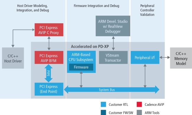
Figure 3
Solution to SoC validation challenges enabled by acceleration and AVIP (Source: Cadence Design Systems – click image to enlarge)
Summary
Integrating and validating embedded firmware and drivers generally requires the software to interact with the RTL. In the past, firmware/driver developers have had to make difficult tradeoff decisions between using RTL simulation and an FPGA prototype. Today, acceleration can be used together with Accelerated VIP to provide a more efficient solution.
That solution delivers the visibility and debug capability of simulation together with performance close to that offered by an FPGA prototype. This combination provides the functionality and performance needed for efficient and effective validation of integrated firmware/drivers/bare metal software.
About the author
Pete Heller is Senior Product Line Marketing Manager for SoC/System level Verification IP at Cadence Design Systems. With more than 20 years of industry experience, he has played a key role in growing Cadence’s VIP business. Heller holds both a BA in Computer Science as well as an MBA from Indiana University’s Kelley Graduate School of Business.
Contact
Cadence Design Systems, Inc.
2655 Seely Avenue
San Jose
CA 95134
USA
T: +1 408 943 1234
W: www.cadence.com


Try out the entire Cadence VIP portfolio for yourself. AXI, OCP, USB 3.0, PCI Express, etc. Just click here, and try it out for yourself on the cloud.