Rapid design flows for advanced technology pathfinding
The paper describes several innovative modifications to standard design flows that enable new device technologies to be rapidly assessed at the system level. Cell libraries from these rapid flows are employed by a design flow description language (PSYCHIC) for the exploration of highly speculative ‘what if’ scenarios. These rapid design flows are used to explore the performance of two competing 15nm technologies in a system L2 cache controller and a PSYCHIC analysis of statistical timing variations in a 45nm memory concentrator.
Introduction
The complexity of current design flows makes it extremely time-consuming to evaluate new device technologies in terms of the parameters that designers need (e.g., clock rate, die area, battery life). The process can take months. This research describes several simplifications to standard design flows that enable extremely short experiment turn-around times—often less than a day—while maintaining reasonable timing accuracy (better than 10%).
This approach is illustrated using two use-case examples. In the first example, the impact of two competing 15nm technologies on the clock-rate versus area trade-off of a large block of intellectual property (IP) is analyzed. In the second example, rapid design flows are then coupled to a design flow description language to enable unique experiments at the 45nm node that directly link process-level variability to timing variations, without recourse to perturbations of device model parameters.
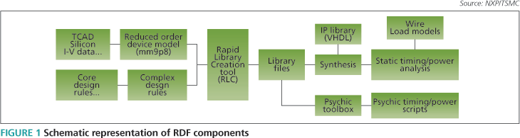
Rapid design flow components
The components of an RDF are shown in Figure 1. Transistors incorporating new materials, architectures and transport mechanisms are designed using Technology Computer Aided Design (TCAD) tools and embedded in the RDF using a model designed to be extracted from only six I-V curves, with eight model parameters.
beta gain factor for one um wide device
vt0 threshold voltage at zero back-bias
m0 sub-threshold slope
gam0 drain-induced threshold shift for zero gate bias
gam1 drain-induced threshold shift for large gate bias
the1 mobility reduction due to vertical field
the3 mobility reduction due to lateral field
rs source/drain series resistance
Although simple, the RDF model maintains the ability to model deep submicron device non-idealities, such as DIBL, velocity saturation, reduced sub-threshold slope and series resistance. Such dramatic model simplification is possible because the dominant pole (i.e., RC constant) of the standard cell frequency response is given by the product of the cell output resistance and the distributed interconnect capacitance. Only the DC properties of the device/cell then need to be modeled accurately [1].
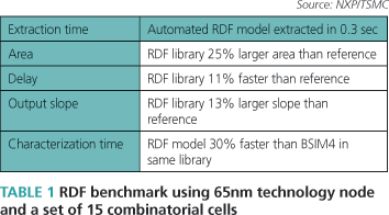
Table 1 summarizes the main results of a benchmarking exercise at the 65nm node, to compare a fully automated RDF-generated library with a commercially produced library. For this comparison, the RDF model was extracted from I-V curves generated from a 65nm BSIM4 model, and design rules for cell layout were generated automatically from the specifications for the lithography tools used at that node.
We observed that 10% timing accuracy was maintained at the cost of a 25% increase in cell area due to the automated cell compaction procedures. A similar exercise at the 45nm node also showed an area penalty of approximately 25%, indicating that the cell area off-set is predictable and node-independent. Although a significant 30% advantage in run-time is observed, the real benefit of the RDF model is the rapid extraction time, 0.3s. This is exploited in the last section of the article.
Coupling to standard synthesis/timing flows
It is anticipated that at the 15nm node, die area will be more important than processing speed. An RDF was therefore used to calculate the area of a system L2 cache controller [2] (approximately 400,000 cells) at constant clock rate, using two competing 15nm technologies. The first was a fully depleted SOI (FDSOI) technology, and the second was a III-V NMOS/Ge PMOS technology.
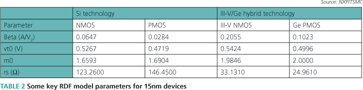
In both cases, the RDF model was based on a bulk CMOS device and therefore the extracted parameters are empirically rather than physically based. Table 2 lists a selection of extracted parameters for each device. The predicted trade-offs between the area and clock rate for the two technologies are shown in Figure 2, where the III-V/Ge library implements the controller in half the area of the FDSOI library at a clock rate of 3GHz.
A design flow description language
For even more rapid technology assessment scenarios, we have developed a design flow description language, called PSYCHIC. This is implemented as a set of functions in a Matlab toolbox (Table 3).
The PSYCHIC approach relies on the use of defined functions to construct custom scripts, tailored to each modeling problem, rather than develop a single compiled program. Here is the script for emulating the static timing of the critical path within the system L2 cache controller.
% STA script for path from system L2 cache controllertech = GaAsGeTech ; % imported technology informationlib = GaAsGeLib2 ; % imported 15nm III-V/Ge RDF librarylogicDepth = 9 ; % number of cells in timing pathslew = zeros(1,logicDepth) ; % starting transition timesdelay = zeros(1,logicDepth) ; % starting delaysM = 630 ; N = 630 ; % rows and columns of cellsheight = GaAsGeLib2.INVD1.height ; width = height ; % square cellspeff = 0.8 ; reff = [0.0 0.7 0.7 0.7 0.7] ; % set place\route efficiencytc = 3 ; tn = 2 ; % set terminals per cell and net% calculate average wire length within arraylav = savlength(height,width,preff,reff,tc,tn,tech) ;% convert to capacitancecload = cint(2,lav,tech).*ones(1,logicDepth) ;initSlew = 0 ; % first input transition time[delay(1),slew(1)]=timing(GaAsGeLib2.DFCND1,cload(1),initSlew,) ;[delay(2),slew(2)]=timing(GaAsGeLib2.INVD1,cload(2),slew(1)) ;[delay(3),slew(3)]=timing(GaAsGeLib2.AN2XD1,cload(3),slew(2)) ;[delay(4),slew(4)]=timing(GaAsGeLib2.ND3D2,cload(4),slew(3)) ;[delay(5),slew(5)]=timing(GaAsGeLib2.NR2D1,cload(5),slew(4)) ;[delay(6),slew(6)]=timing(GaAsGeLib2.INVD2,cload(6),slew(5)) ;[delay(7),slew(7)]=timing(GaAsGeLib2.NR2D1,cload(7),slew(6)) ;[delay(8),slew(8)]=timing(GaAsGeLib2.NR2D1,cload(8),slew(7)) ;[delay(9),slew(9)]=timing(GaAsGeLib2.IOA21D2,cload(9),slew(8)) ;pathDelay = sum(delay) ;
Note that the script itself is node-independent, and technology and library information are ‘fire-walled’ within separate tech and lib files, respectively.
The toolbox makes it easy to couple RDF libraries with new design flow concepts such as statistical static timing analysis. In this context, the output load, input and output transition times and delay parameters of the timing function are not single values but probability density functions. Scripts based on this approach have been used to assess the impact of process-level variability on critical path timing.
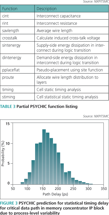
Variations were introduced into a TCAD model of a 45nm device by varying the gate insulator thickness (?EOT=1Å) and gate length (?L=3nm), in order to produce 50 sets of NMOS and PMOS I-V curves (five hours processing time). RDF device models were then extracted for each device variant (extraction time 30 sec). Fifty libraries were then generated and characterized (total time one day) and imported into PSYCHIC. Statistical static timing experiments were carried out on the slowest timing path extracted from a 45nm memory concentrator block within a multimedia processor SoC. Figure 3 shows the results. The timing histograms for each cell in the path were convolved to produce the overall path delay.
This approach allows fundamental experiments to be performed on the effects of process-level variability on system-level timing, and avoids issues associated with varying individual parameters within a single compact model to generate timing statistics [3].
Conclusions
Benchmarking with commercially generated libraries shows that 10% timing accuracy and 30% run-time gain can be maintained with RDF libraries at the cost of a consistent, node-independent 25% cell area penalty. As an example, this approach was used to analyze the clock rate-area trade-off for a system L2 cache controller implemented using two competing 15nm technologies.
In order to explore more speculative ‘what if’ scenarios and to avoid costly synthesis and timing tools, a design flow description language was developed. Scripts written in this language were shown to reproduce critical path timing data from, for example, Cadence Encounter to 2% accuracy. The unique capabilities of RDF libraries and the ease of implementing new PSYCHIC functions were employed to analyze statistical timing variations in a 45nm memory concentrator.
References
- P. Christie, et al., Proc. IEDM (2007).
- P. Stravers, et al., Proc. Int. Sym. VLSI-TSA (2001)
- C. Visweswariah, Proc. Design Automation Conference (2003)
NXP-TSMC Research Center
Kapeldreef 75
B-3001
Leuven
Belgium
NXP Semiconductors
High Tech Campus
5656 AE Eindhoven
The Netherlands
W: www.nxp.com
W: www.tsmc.com