An ISO 26262 approach to meeting the cost, quality, reliability, and integration needs of automotive ICs
Meeting ISO 26262 standards for automotive safety means applying a consistent approach throughout the design process. Here’s how to start.
Today’s cars include safety systems such as anti-lock braking, air bags, traction control, and electronic stability control. Next-generation advanced driver assistance systems use more complex combinations of cameras and radar to sense, identify, and alert drivers of hazards.
The embedded systems needed to gather, analyze and act upon the sensor data must be built with components that have been designed, made, tested and certified to rigorous functional safety standards, such as ISO 26262 and IEC 61508. These standards require that safety-critical systems minimize the risk of failure by eliminating or reducing the risk of systematic and random errors.
Working with ISO 26262
The ISO 26262 functional safety standard defines automotive safety integrity levels (ASILs) to define the potential risk of an automotive system (Figure 1). The risk is defined in terms of the severity of a failure, the probability the failure will result in a safety hazard, and the probability that harm can be avoided when a hazardous condition occurs.
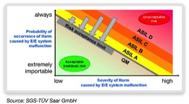
Figure 1 ISO 26262 categorization of risk potential. (Source: SGS-TÜV Saar GmbH)
ISO 26262 says that the software tools used to design and test the ICs used to build high-risk safety-critical systems (at ASIL C or D) must themselves be qualified to ensure that they don’t introduce errors or fail to detect errors.
Tool qualification involves assigning a Tool Confidence Level, defining the qualification plan, defining and verifying the operational requirements, providing an analysis of how the design and test tools perform, and maintaining tool artifacts (such as documentation, flows, bugs that could impact safety, and workarounds for those bugs).
Synopsys has qualified its automotive IC test solution for ASIL D designs, and they have been certified by SGS-TÜV Saar GmbH, an independent accredited assessor. Users need only follow the instructions provided in each tool’s safety documentation, and include the tool’s certificate as part of the safety case for the design.
The tools also enable designers to focus on meeting the quality, reliability, cost and integration requirements of automotive ICs.
Meeting quality requirements
Suppliers want the ICs they use in safety-critical systems to have the highest possible quality, which they specify within an operating range. An IC vendor will design a part to operate to a specification, and will guarantee that most parts will operate within a band defined by a lower spec level (LSL) and an upper spec level (USL). The number of parts that fall outside this band will depend on the standard deviation of the manufacturing process from its target (see Figure 2).
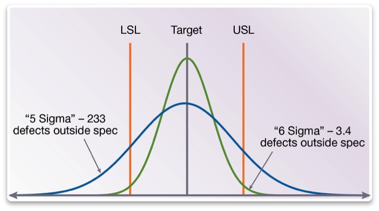
Figure 2 A 5 sigma quality level implies 233 defective parts per million, while a 6 sigma level guarantees fewer than 4 such parts
Process variations and random defects can change the delay and leakage behavior of logic gates. A lithography defect may cause excessive coupling between two electrical nodes, adding enough delay to cause a design to fail under certain conditions. Testing strategies need to achieve very high coverage of subtle defects to ensure the required defective parts per million (DPPM) levels. Figure 3 shows DPPM levels for automotive parts at various sigma values, and an estimate of the corresponding defect coverage levels, based on defect models and a manufacturing yield of 80%.
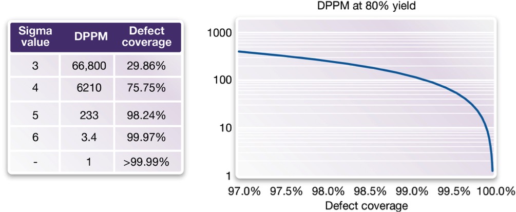
Figure 3 The relationship between defect coverage rates and resultant DPPM levels (Source: Synopsys)
Achieving a defect rate of just 1 DPPM requires more than 99.99% defect coverage. This is a challenge, but possible if the ATPG tool takes a design’s timing and physical characteristics into account. Synopsys’ TetraMAX Automotive ATPG tool generates test programs that target a wide range of silicon defects by using advanced fault models that exploit the links between Synopsys’ design and analysis tools to capture timing and physical information. For example, Synopsys’ slack-based, cell-aware ATPG can achieve ultra-high defect coverage by targeting small delay defects inside cells, using timing information generated by Synopsys’ PrimeTime signoff solution and HSPICE circuit simulation tools (Figure 4).
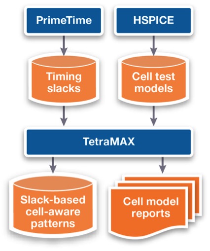
Figure 4 The TetraMAX Automotive ATPG flow for slack-based cell-aware test uses timing slack data from PrimeTime and timing information from HSPICE to target defects within cells (Source: Synopsys)
Meeting reliability requirements
To meet the ISO 26262 automotive functional safety standard, ICs must be able to perform self-tests in service. Synopsys has tools that enable the design of in-system and power-on self-test strategies for memory and logic.
DesignWare STAR Memory System automates the test, repair, and diagnostics of embedded and external memories.
DFTMAX LogicBIST synthesizes logic for in-system and power-on self-test. It is synthesis-based, and part of the wider Design Compiler RTL offering, which can co-optimize the timing, power, area and routability of both test and functional logic.
The Synopsys logic BIST flow (Figure 5) starts with either RTL or a netlist, synthesizes logic BIST and creates a testbench. An intermediate step programs data from TetraMAX Automotive ATPG into the design, once final pattern counts and coverage have been determined. The self-test strategy is based on generating pseudo-random patterns on chip. These patterns are different to those that TetraMAX generates for manufacturing tests. Links between DFTMAX LogicBIST, DFTMAX Ultra compression, and TetraMAX speed up tasks such as calculating the seed and signature, and analyzing and inserting test points.
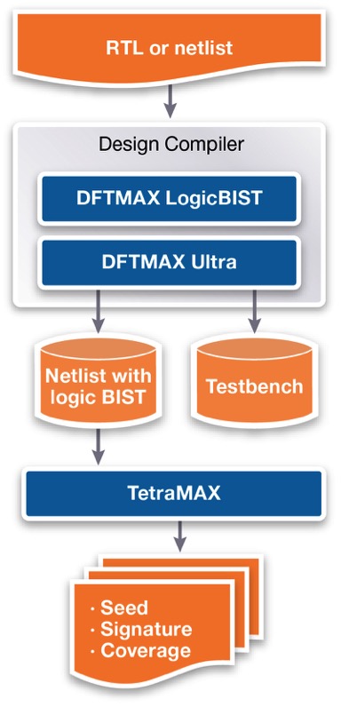
Figure 5 DFTMAX LogicBIST is built into Design Compiler to optimize timing, power, and area for both test and functional logic (Source: Synopsys)
For manufacturing test, DFTMAX LogicBIST inserts logic BIST registers into scan chains along with the functional logic. Scan and compression modes are both supported to ensure that an area-efficient logic BIST architecture can be applied to local, safety-critical circuitry, while a more broadly applied manufacturing strategy can address the top level of the circuit.
Addressing cost effectiveness
Users of automotive ICs want the highest quality to ensure functional safety, and competitive prices. It’s up to designers to find cost-effective ways to deliver greater defect coverage and fewer test escapes, while controlling the growth of test data volumes, time and costs associated with running the extra patterns needed to achieve that coverage.
This challenge is compounded by the fact that fewer pins are being allocated for test. This is happening for a number of reasons. There’s increasing use of mixed-signal designs with small form factors and few digital pins. There’s growing uptake of test-cost reduction techniques such as multisite test, which uses very few test pins to test multiple chips simultaneously. And core-based test methodologies are being introduced into SoCs.
Synopsys’ DFTMAX Ultra is designed to achieve higher compression using fewer pins. The architecture is optimized to provide TetraMAX with maximum flexibility to manage unknown logic values to improve ATPG coverage, increase compression efficiency, and enable accurate fault diagnostics.
Fast SoC test integration
The final challenge is integrating all the memory, logic, and AMS/IP cores and efficiently testing the SoC. Traditional methods for core integration and pattern porting take time and can be prone to errors. Synopsys’ DesignWare STAR Hierarchical System automatically creates a hierarchical IEEE 1500 network on-chip to access and control all the cores at the SoC level (Figure 6). It uses the network to port core-level patterns to the SoC level, where testing can be scheduled based on test time or test power considerations. STAR Hierarchical System is compliant with the IEEE standard 1687, which allows re-use of embedded test instruments for system-level debug.
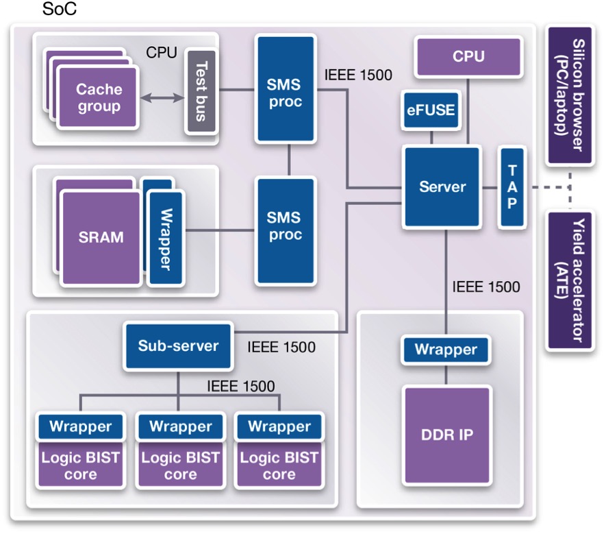
Figure 6 DesignWare STAR Hierarchical System (Source: Synopsys)
IP for standard mixed-signal interfaces such as PCIe, USB 3.0, HDMI, and other SERDES interfaces contains BIST for running loopback tests to view analog waveforms during test. The Synopsys DesignWare SERDES IP supports this facility, and can have its analog output trimmed based on the waveforms. STAR Hierarchical System accesses these cores over the IEEE 1500 infrastructure, coordinates the IP test, and supports trimming using on-chip fuses.
For custom mixed-signal blocks, STAR Hierarchical System uses IEEE 1500 infrastructure to control and observe the digital signals of the blocks.
The tool also has offers process and clock-monitoring capabilities. Clock integrity is important to automotive IC customers, and so a typical automotive IC may include many process monitors. The ability to measure the clock frequency and duty cycle without needing an extra, higher-frequency clock addresses these requirements. STAR Hierarchical System also enables insight into wafer-level process variations using a ring oscillator structure, defined in RTL, that is foundry and process agnostic.
Further information
- Webinar with STMicroelectronics
- Low DPPM Testing White Paper
- DFTMAX LogicBIST datasheet
- DFTMAX Ultra datasheet
Author
Chris Allsup is a senior staff technical marketing manager in Synopsys’ synthesis and test group, has more than 20 years combined experience in IC design, field applications, sales, and marketing. He earned a BSEE degree from UC San Diego and an MBA degree from Santa Clara University. Allsup has authored numerous articles and papers on design and test.
Company info
Synopsys Corporate Headquarters 690 East Middlefield Road Mountain View, CA 94043 (650) 584-5000 (800) 541-7737 www.synopsys.comSign up for more
If this was useful to you, why not make sure you’re getting our regular digests of Tech Design Forum’s technical content? Register and receive our newsletter free.