Migration of the Cell Broadband Engine to 45nm SOI
The paper describes some of the main challenges in the latest process shrink for the Cell Broadband Engine, developed jointly by IBM, Sony and Toshiba. The authors show how the move from a 65nm to a 45nm SOI process was achieved by concentrating on four primary goals:
- automating the migration;
- setting a 30% power reduction target;
- setting a 30% area reduction target; and
- promoting design for manufacturability (DFM).
The extensive use of IBM’s in-house developed tool, Migration Assistant Shape Handler, is also described.
The migration of the Cell BE involved collaboration across several sites within the three participating companies. Details of the authors and their locations appear at the end of the article.
The paper describes the challenges of migrating the Cell Broadband Engine (Cell BE) [1, 2] design from a 65nm silicon-on-insulator (SOI) [3] process to a 45nm twin-well CMOS technology on SOI with low-k dielectric (k = 2.4) and 10 copper metal layers [4].
The 45nm technology offers dual-gate oxide thicknesses of 1.16nm and 2.5nm for, respectively, 1.0V and 1.5V nominal power supplies. Thicker oxide devices are used in analog circuits.
To guarantee the proper operation of existing gaming software, the exact cycle-by-cycle machine behavior—including operating frequency—from earlier process nodes must be preserved.
We placed the main focus of the migration on four goals:
- automated design migration where possible;
- a 30% power reduction;
- a 30% area reduction; and
- design for manufacturability (DFM) improvements.
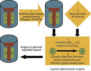
Figure 1. MASH system flow. Source: IBM
As the design rules across the various process technologies were relatively compatible, we took advantage of automated migration for the bulk of the Cell BE circuit blocks. Circuits were then manually fine-tuned for timing, noise tolerance and design robustness.
We took a different approach for the memory and analog circuits. Analog circuits do not scale well because of the area required for decoupling capacitance. The I/O area—especially the area for C4 bumps—dictated chip dimensions since the same number of I/O signals was required and the C4 pitch did not scale from the previous technology.
Since digital circuits occupy the bulk of chip area, it is crucial that they are migrated effectively. The original digital circuits in 65nm consisted of three types of components: parameterized cells, common leaf cells (flip-flop and local clock buffer) and custom cells.
The migration of parameterized cells was done through software. An IBM tool called Migration Assistant Shape Handler (MASH) [5] is applied to the common leaf cells. Its typical flow is illustrated in Figure 1. MASH first shrinks the shapes according to the scale factor between technologies. Second, MASH corrects as many design rule violations in 45nm as possible with minimum layout perturbations, and the remaining violations are repaired manually. The pin locations for these cells are fixed and scaled only in size. Metal blockage changes are minimized to reduce the effect on higher design levels.
Hierarchical migration is performed in two phases. The first phase includes placing scaled leaf cells at scaled coordinates and scaling any remaining shapes. The second phase applies MASH to remove design rule violations.
Using this design migration methodology, we shrank the chip size by 34% against its dimensions at 65nm. Figure 2 shows the dimensions of Cell BE and its major partitions in three technologies.
We took as much advantage of the automated approach as possible by applying it to smaller memory array blocks and then tuning circuits manually.
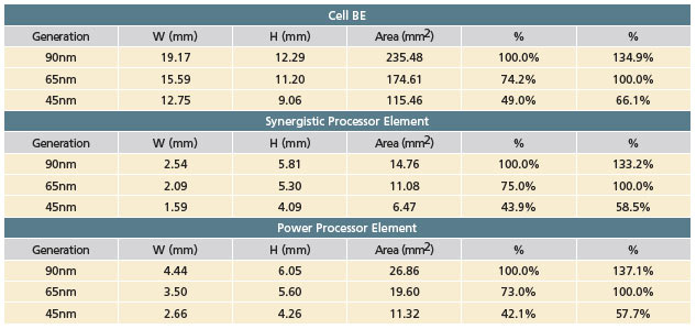
Figure 2. Cell BE dimensions and its major partitions in three technologies. Source: IBM/Sony/Toshiba
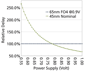
Figure 3. Relative FO4 delay of 45nm with respect to that in 65nm @ VDD = 0.9V. Source: IBM/Sony/Toshiba
As the SRAM cell size shrank to 0.404um2 at 45nm from 0.7um2 at 65nm, we addressed concerns over cell stability due to process variability [6] by using a separate array power supply (VCS).
Lowering the main power supply (VDD) is critical for reducing the chip power consumption. However, we could not lower VCS by the same amount as VDD because of SRAM cell stability requirements. A larger gap between VDD and VCS can lead to boundary issues, such as leakage from one power supply to the other. In response, we included a level shifter at the voltage boundaries in the wordline and pre-charge signal drivers. Figure 5 shows the combined wordline driver and level shifter.
Since gaming applications require the 45nm Cell BE to operate at the same frequency as the 65nm and 90nm designs, we used device performance improvements in 45nm to reduce chip power by lowering VDD. The 65nm Cell BE operates at a VDD of 0.9V. Figure 3 shows the relative FO4 delay at 45nm at various VDD with respect to that of 65nm at VDD = 0.9V. The equivalent delay is maintained by lowering VDD by roughly 100mV. Hence, this becomes the 45nm timing corner power supply. The 45nm Cell BE remains an 11FO4 design at 45nm as at 65nm.
The remaining power reduction techniques we implemented at 45nm were:
- converting dynamic circuits (some dynamic programmable logic arrays and a dynamic carry generator) to a full static CMOS implementation wherever possible;
- reducing the use of lower-threshold voltage devices (regular Vt) from 2.4% to 0.5% for PMOS and from 2.9% to 0.7% for NMOS, respectively;
- retuning local clock and timing control signals to remove signal collisions and high signal slew rates; and
- re-optimizing the footprint of power C4 bumps.
Additional power C4 bumps were placed in the high current areas of the 45nm Cell BE to reduce the IR drop in the vicinity. This led to an improved VMIN, helping to reduce the overall chip power.
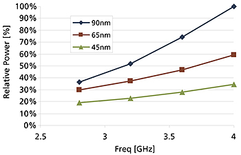
Figure 4. Simulated relative power of Cell BE at various frequencies in three technologies. Source: IBM/Sony/Toshiba
Figure 4 (p. 38) shows the relative power of Cell BE in three technologies at different frequencies, using a Cell BE power model at the same condition of nominal process, 90°C, and the same workload. The power supply is adjusted to a minimum value where the chip is still functional at a particular frequency. The VCS C4 supply is fixed at 1.25V for 65nm and 1.15V for 45nm. We used PICA [7] measurements, Vt spread measurements in the 65nm Cell BE, and model prediction in the 45nm Cell BE to improve the power model accuracy.
We relied on in-house yield-checking software to identify the areas for DFM improvement. Design modifications were done manually and by MASH. We relied on MASH for systematic improvements such as redundant contact placement, metal short edge removal, diffusion short edge removal and n-well optimization for stress effect.
The yield-checking software is basically a design rule checker with stricter rules. The yield-checker determines a yield score by the number of violations against the number of total occurrences.
When the score reaches a predefined threshold value, the checking item passes successfully.
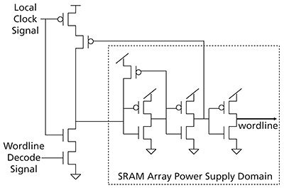
Figure 5. The composite circuit of level shifter and wordline driver. Source: IBM/Sony/Toshiba
Critical functional blocks are reviewed by applying lithography simulation and critical area analysis, in addition to layout recommendations for yield, performance and device matching.
We have described the migration of the Cell BE design from 65nm to 45nm using a mostly automated approach. Cycle-by-cycle machine behavior was preserved. The chip power was reduced by roughly 40% and the chip area was reduced by 34%.
References:
(1) B. Flachs et al., “A Streaming Processor Unit of a CELL Processor,” ISSCC Dig. Tech. Papers, pp. 134-135, Feb. 2005.
(2) D. Pham, S. Asano, M. Bolliger, et al., “The Design and Implementation of a First-Generation CELL Processor,” ISSCC Dig. Tech. Papers, pp. 184- 185, Feb. 2005.
(3) W.-H. Lee, A. Waite, H. Nii, et al., “High Performance 65nm SOI Technology with Enhanced Transistor Strain and Advanced-Low-K BEOL,” IEDM Dig. Tech. Papers, pp. 61, Dec. 2005.
(4) S. Narasimha, K. Onishi, K. Nayfeh, et al., “High Performance 45nm SOI Technology with Enhanced Strain, Porous Low-BEOL, and Immersion Lithography,” IEDM Dig. Tech. Papers, pp. 689, Dec. 2006.
(5) F.-L. Heng, Z. Chen, G. Tellez, “A VLSI Artwork Legalization Technique Based on a New Criterion of Minimum Layout Perturbation,” Proc. ISPD, pp. 116-121, Apr. 1997.
(6) J. Pille, C. Adams, T. Christensen, et al., “Implementation of the Cell Broadband Engine in 65nm SOI Technology Featuring Dual Power Supply SRAM Arrays Supporting 6GHz at 1.3V,” ISSCC Dig. Tech. Papers, pp. 322-323, Feb. 2007.
(7) F. Stellari , P. Song, J. Tsang, et al., “Testing and Diagnostics of CMOS Circuits Using Light Emission from Off-State Leakage Current,” IEEE Trans. Electron Devices, vol. 51, no. 9, pp. 1455-1462 Sept. 2004.
Authors
This paper was written by: O. Takahashi1, C. Adams2, D. Ault1, E. Behnen1, O. Chiang1, S. R. Cottier1, P. Coulman1, J. Culp3, G. Gervais1, M. S. Gray4, Y. Itaka5, C. J. Johnson2, F. Kono5, L. Maurice1, K. W. McCullen4, L. Nguyen1, Y. Nishino6, H. Noro5, J. Pille7, M. Riley1, M. Shen1, C. Takano6, S. Tokito6, T. Wagner3, H. Yoshihara6.
- 1IBM, Austin TX
- 2IBM, Rochester, MN
- 3IBM, Hopewell Junction, NY
- 4IBM, Essex Junction, VT
- 5Toshiba America Electronic Components, Austin, TX
- 6Sony Computer Entertainment of America, Austin, TX
- 7IBM, Boeblingen, Germany