Top-level MCMM closure for a multi-million-gate design
STMicroelectronics in Greater Noida, India recently completed an Omega2 set-top-box decoder IC targeted at HDTV markets. This article discusses how ST used Mentor Graphics’ Olympus-SoC software to address the closure challenges presented by a very large design. It describes how the design team used the tool suite’s chip assembly, concurrent multi-corner multi-mode (MCMM) analysis and optimization, and chip finishing capabilities to reduce design iterations, cut time-to-tapeout and optimize the overall resource requirements.
Design description and design flow challenges
The Omega2 STMicroelectronics chip (Figure 1) discussed in this case study is a member of a family of HD set-top box decoders that integrate an MPEG-4 decoder. The SoC is implemented in a 65nm process that is then shrunk to 55nm. It contains 4.5M instances (18M gates), 311 macros, three CPU hard cores and 640 I/Os.
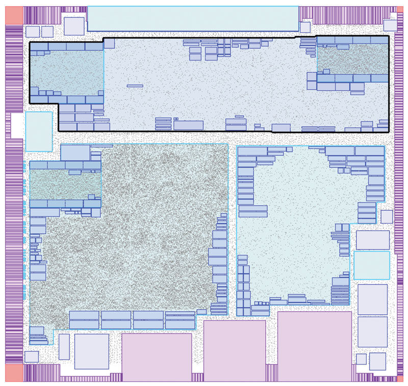
Figure 1
The STMicroelectronics Omega2 set-top box chip. Source: ST
The top-level SoC physical hierarchy consists of three partitions and 360 functional pads. There are 125 clock domains. For design closure, there were four operating modes, each with three process corners. The main challenges in realizing the design centered on improving the design closure process without sacrificing chip performance.
Our existing flow imposed a hierarchical timing closure methodology in which the chip was partitioned, and then the partitions were implemented and instantiated at the chip level as abstraction models for top-level timing sign-off. Using block abstractions at the chip level proved to be inefficient for converging on timing closure. It took many traditional ECO iterations to fix timing violations on inter-block paths, and that was especially true for this design because of the number of mode/corner combinations we had to close.
We wanted to optimize the full chip in a flat mode as opposed to a hierarchical one. We also wanted to optimize for all the mode/corner combinations required for sign-off. Because of the huge design size, we had not been able to visualize the timing of the full chip flat in a physical design environment. This meant that we were also leaving some performance untapped because we were forced to accept wider timing margins.
Finally, we wanted to reduce the time, compute resources and engineering hours spent in timing closure iterations. One engineer was dedicated to the top-level work, and three engineers (one for each partition) performed the timing and signal integrity (SI) closure iterations for each partition. In summary, the main challenges included:
- optimizing the top-level timing closure cycle-time;
- securing MCMM design closure capabilities;
- addressing existing tool capacity; and
- avoiding the inefficient use of engineering resources.
One problem with our previous top-level timing closure process had been that timing models used during chip optimization were not accurate enough to close chip-level timing. We had to rely on pessimistic timing budgets allocated during chip budgeting, which often caused I/O and inter-partition timing violations. Also due to the timing models, chip-level clock tree synthesis could not be done flat to meet very precise skew and latency targets. It required iteration during the timing closure phase.
Handling MCMM timing in our flow was also a challenge. The block implementations were done for best case/worst case timing in two modes, but sign-off timing had to be met for several other modes and four corners. Therefore, we usually found some ‘cross corner’ or ‘cross mode’ violations during sign off that were not seen during the implementation. We could fix these by undertaking ECOs, but this was obviously expensive from a schedule perspective.
In our previous flow, full chip static timing analysis (STA) required a separate extraction run for each of the four design corners, then an analysis would be run for each mode/corner combination. The timing results were manually analyzed and fixed in each partition, and checked with chip-level STA. We then performed full extractions again and re-analyzed. We often found that fixing a violation in one timing scenario would cause a new timing violation in another. It sometimes took several iterations, the efforts of multiple engineers, and several weeks to close timing under this iterative method.
Toward a new design flow
We needed a way of improving the MCMM closure, allowing full-chip optimization, and performing the chip assembly that incurred fewer sign-off iterations and expended fewer resources. We turned to the Mentor Graphics Olympus-SoC place and route system.
Because the project had already started, we needed something that would cause the least disruption to the existing methodology. To minimize the risk associated with changing the design flow completely, we adopted Olympus-SoC to assist in the specific areas of chip-level assembly, MCMM optimization, timing closure and chip finishing.
Tool setup and timing correlation
The software uses industry standard input and output formats (e.g., LEF, DEF, Verilog), so we were able to use in-house libraries that were already part of our design kits. We had no problem reading in the block/partition DEF and Verilog files and in viewing the entire chip in a single flat representation.
We performed timing correlation between our sign-off tool and Olympus-SoC and the results showed a very close match, with Olympus within 10% of the sign-off reference slack calculations. Figures 2a and 2b show the best case and worst case timing correlation graphs.
Full chip optimization
Olympus-SoC was able to load and process our full 18M-gate design flat, while maintaining the design’s logical hierarchy. We liked the fact that timing modeling of partitions/blocks was not a requirement for chip assembly. We need the freedom to choose which blocks to abstract, depending on the top-level paths and the level of accuracy needed. For example, we might abstract a block that is cloned heavily, while a block that is not cloned does not need to be abstracted giving us greater accuracy in chip-level timing measurements. This is particularly important when optimizing inter-block paths because the tool can see the entire path end-to-end. Figure 3 shows the chip with an inter-block path highlighted.
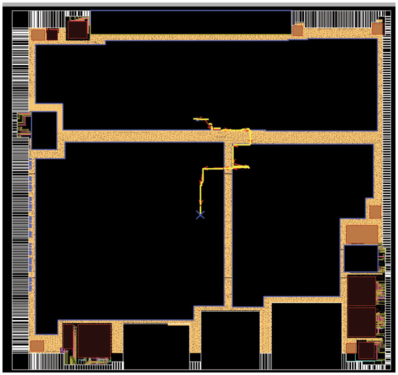
Figure 3
Full chip with an inter-block path highlighted. Source: ST
Olympus-SoC allowed us to optimize the design at the top level (including I/Os) and at the block level at the same time, full flat. Because the block-level boundaries were maintained, any optimization-logic changes made to the blocks during flat optimization were directly updated inside the blocks. This type of dynamic update is only possible in situ with a tool that has the capacity to support a flat full-chip view. Figure 4 (p. 38) shows the Olympus-SoC capability to optimize partition to I/O paths.
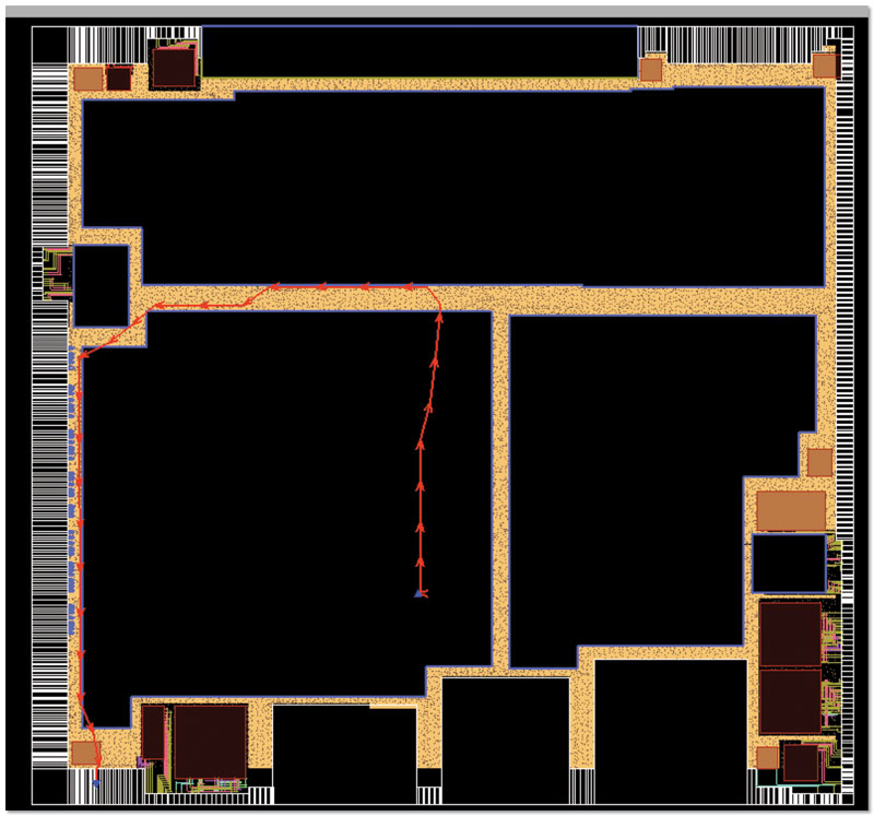
Figure 4
Full chip with partition-to-pad path highlighted. Source: ST
For the MCMM optimization, we set up the mode-corner combinations information at the beginning, and the tool quite smoothly and automatically optimized all the relevant scenarios.
At the start of the top-level flow, we generated a variability report from within Olympus-SoC that showed the initial timing situation for blocks in the full chip context. Table 1 (p. 35) shows the initial variability report before top-level optimization. It shows worst negative slack (WNS), total negative slack (TNS), worst hold slack (WHS), and total hold slack (THS), for six different variability scenarios after optimization.
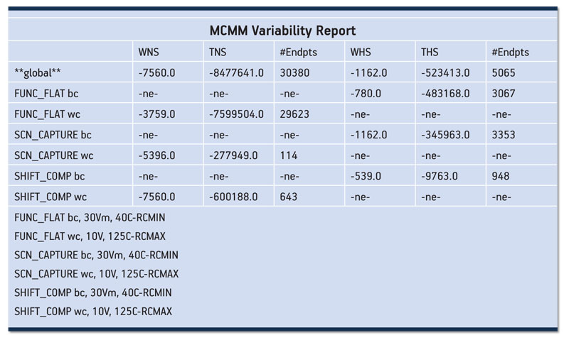
Table 1
Variability report before top-level optimization. Source: ST
We then ran full chip optimization in Olympus-SoC, performed a single extraction that covered all four corners, and analyzed the results in the sign-off timer. All ECOs were done in a full-flat context in Olympus-SoC, followed by a single re-extraction and re-analysis. This flow gave better optimization results, particularly for inter-partition (or inter-block) paths, and greatly reduced the number of timing ECO cycles to achieve full-chip closure.
The total number of ECO iterations needed with Olympus-SoC was significantly less than with our previous flow. Table 2 shows the variability report generated after the last top-level optimization. It shows the same metrics as before for six different variability scenarios. After closing the timing, we used Olympus-SoC for chip finishing and final streamout of the GDSII.
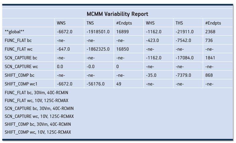
Table 2
Variability report after top-level optimization with Olympus-SoC. Source: ST
Potential improvements
We derived significant benefits from our use of Olympus-SoC in the flow for the Omega2. However, the introduction of any new tool into a flow always presents some challenges. For example:
- We were not able to close timing for two tricky clock domains. This was because of a floor-planning limitation, however, the tool could have given some pointers or metrics to indicate the extent of the problem it had encountered.
- We found that some pad delays differed between the sign-off tool and Olympus-SoC. This issue has been fixed. For some of the pads, Olympus-SoC’s timing calculations were slightly more optimistic than those from the sign-off tool, and for some I/O paths Olympus-SoC’s timing was slightly more pessimistic. In response, we masked all I/O paths and violations for some of the modes, which were later fixed during an ECO loop.
- For manual last-mile DRC fixing, we thought that the wire editing function could have been easier to use and more dynamically aware of violations caused during editing. These observations have subsequently been addressed by the Olympus-SoC development team.
- During stream-out, the tool had some problems with the uniquification process and in understanding the empty GDS files within hard macros. This was fixed before the final GDSII stream out.
Results
The use of Olympus-SoC for full-chip optimization and chip finishing gave us significant improvements compared to our previous approach to timing closure. It was easy to set up, and the correlation with the sign-off timing tool was good. Because of its high capacity, relatively small memory footprint, MCMM timing closure capability, efficient multithreading and accuracy, we reduced timing closure on the Omega2 from two weeks to less than three days. Notably, we saved time during sign-off by being in a position to run full-chip, MCMM optimization that significantly reduced the number of ECO iterations.
Given our experience with Olympus-SoC on our HD set-top box decoder, we plan to use this tool extensively for futures designs.
Acknowledgements
The authors wish to recognize the contributions made to this project by their colleagues at STMicroelectronics, Vivek Sinha, Sachin Mathur, Suman Gupta, Azad Singh, Mohit Verma and Deepak Garg, and by Mentor Graphics’ Ajay Mishra.
STMicroelectronics Pvt. Ltd.
Plot 1
Knowledge Park III
Greater Noida – 201308 (U.P.)
India
T: +91 120 2352999
W: www.st.com