The art of low-power physical design
The architectures that underpin today’s traditional place-and-route tools are showing their age, largely because their static timing analysis engines cannot handle more than two mode/corner scenarios. Thus limited, the software struggles to effectively implement low-power design techniques beyond such established concepts as clock gating and multiple threshold voltages.
Designers run into difficulties when trying to exploit more advanced techniques such as designing for power in a multi-corner, multi-mode (MCMM) context, incorporating multi-voltage flows, and implementing power-efficient clock trees. These advanced techniques are becoming increasingly vital to successful design as process nodes shrink. The article outlines how efficient MCMM techniques are becoming available and can help designers meet their low-power targets.
One of today’s biggest design challenges lies in handling the complexity inherent in effective power management. Whether your goal is the reduction of on-chip power dissipation or the extension of battery life, power stands alongside timing as a critical dimension to be optimized during physical design. At advanced process nodes, nearly all designs must incorporate some kind of power-saving strategy. But in seeking to deploy increasingly sophisticated low-power techniques, engineers face huge implementation hurdles in terms of cost, performance, and time-to-market. Current place-and-route (P&R) tools are severely limited by aging architectures and the inability of their core static timing analysis (STA) engines to represent more than a couple of mode/corner scenarios.
Most tools support the use of established low-power design techniques (e.g., clock gating to reduce dynamic power, multiple threshold voltages to decrease leakage current), but only across a limited range of mode/corner scenarios. Designers run into difficulties when trying to exploit more advanced techniques such as designing for power in a multi-corner, multi-mode (MCMM) context, incorporating multi-voltage flows, and implementing power-efficient clock trees. This article outlines how to follow some of these more sophisticated strategies without the expected pain.
MCMM timing and power closure
From 65nm onwards, designers have been forced to balance macro-level functional complexity (multiple operational modes) against micro-level process and manufacturing requirements (multiple design corners), all within stringent targets for performance and time-to-market. The demands of low power and signal integrity (SI) exacerbate the timing closure problem as the two fields can have conflicting requirements at certain corners. Reaching the optimum result requires the concurrent analysis and optimization of timing, power and SI interactions across all different modes and corners, a process referred to as multi-corner multi-mode design closure.
The last generation of tools could not handle more than a few mode/corner scenarios at any time. Specifically, the timing and power graph—the most fundamental data structure in any implementation system—was generated from one mode and one setup/hold corner analysis. P&R engines were limited by the data stored in such structures. It is very difficult to do any replacement or retrofitting to overcome this basic architectural limitation, so it is nearly impossible for these aging solutions to efficiently address today’s MCMM-related challenges.
‘Super-mode’ and ‘super-corner’ are strategies that try to compensate for the lack of a true MCMM infrastructure. Ideally though, designers need the ability to capture the circuit behavior for any number of modes and corners dynamically, without impacting memory requirements and runtimes.
Multi-voltage design with MCMM
The use of multiple voltage islands (multi-VDD) is an increasingly common technique used to reduce dynamic power. It allows some blocks to use lower supply voltages than others, or to be completely shut off for certain modes of operation. This presents challenges for physical design.
First, tools need to correctly place and route a design across multiple domains and ensure that the timing and optimization engines honor the multi-voltage domain specifications. Second, a successful multi-VDD implementation requires that MCMM requirements are satisfied in the same run. In essence, each additional voltage island causes the number of timing analysis mode/corner scenarios to double when all the ‘min/max’ voltage combinations are considered (Figure 1). 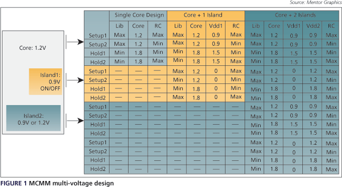
This requires a multi-voltage MCMM implementation system that includes significant architectural and algorithmic enhancements over traditional P&R tools. This approach has been taken in the development of Olympus-SoC from Mentor Graphics (Figure 2).
An industry standard, such as the Unified Power Format (UPF), must be used to setup the implementation and verification specification. The UPF file contains the definitions for power domains and the power state table (PST), and is read alongside library and design data. 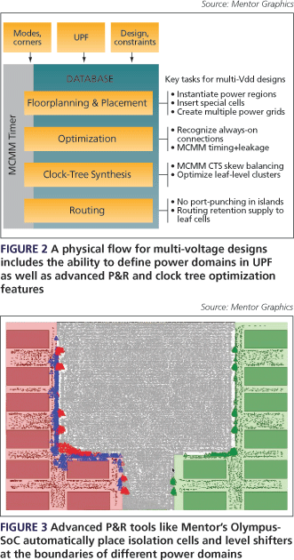
During floorplanning and placement, it is important to correctly floorplan the voltage islands and, where appropriate, insert special cells (e.g., isolation cells, level shifters, power switches, always-on connections and retention cells). The tool should also have a fast placer to group cells into partitions and assign partition pins if needed. Power and ground routing can then create grids for each voltage island.
The tool should provide an easy way to analyze always-on connections, level shifters and isolation cells to ensure they are correctly placed before proceeding with routing. Figure 3 illustrates a basic multi-voltage floorplan with the islands, cells assigned to each island, isolation cells and level shifters clearly marked.
The PST information includes combinations of voltages and power states that are essentially operational modes in a MCMM environment. A concurrent multi-corner, multi-mode, multi-power state analysis and optimization engine can then be used to achieve single-pass closure. During optimization in multi-voltage designs, it is critical that the optimizer respect isolation cells, level shifters and retention registers, only resizing them with equivalent cells. Likewise, always-on buffers must be respected to avoid breaking connectivity and ending up with the dreaded always-off condition.
The router must honor domain boundaries and also handle all the secondary power connections for retention flops and always-on buffers. By default, it should respect voltage island boundaries and route over domains only if specified by the user to either meet timing requirements or to minimize congestion.
The use of a gas station methodology, which allows level nets to cross voltage islands, is becoming a prevalent routing strategy in multi-voltage flows. With the gas station approach, top-level nets can be buffered within shut-off domains using gas stations or islands that are connected to the top-level constant supply voltage.
The router should also contain design-for-manufacturing intelligence so it ‘sees’ and accounts for the manufacturing variations that affect power (especially leakage power) such as on-chip temperature and thickness.
Post-route optimization for multi-voltage designs often uses several techniques that reduce leakage power. These include re-buffering with multiple threshold cells (multi-Vt) and concurrent timing/leakage/area optimization. For the most effective design closure, optimization should be done concurrently across all the corner/mode/voltage scenarios through all steps of the design flow. Without concurrent MCMM optimization, the tool may never be able to resolve conflicting constraints for different mode/corner/power-state combinations.
Low-power MCMM clock-tree synthesis
Any low-power design strategy must pay serious attention to the clock-trees. Clocks are the single largest source of dynamic power usage, and the clock-tree synthesis and optimization stage is a good place to achieve power saving in physical design. Low-power clock-tree synthesis (CTS) strategies include lowering overall capacitance and minimizing switching activity. However, getting the best power results from CTS depends on your ability to synthesize the clocks for multiple corners and modes concurrently.
Clocks present additional challenges at advanced nodes because of sharp increases in resistance that come with smaller geometries. Variation in resistance also increases as wires become more sensitive to manufacturing variations in their dimensions. Figure 4 illustrates the changes in resistance and variations in resistance from 90 to 45nm. Clock-tree synthesis (CTS) gets even more complicated in multi-voltage flows and can have a huge impact on active power dissipation if not implemented correctly. 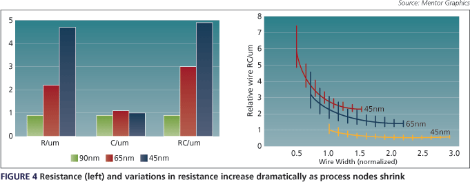
One way to reduce capacitance—and therefore power—is to optimize functional skew across multiple corners based on flop interactions. Most CTS tools balance global skew across all the flops regardless of the clock-tree level they inhabit. Designers then have to manually drive CTS to balance the sinks correctly. If the CTS engine can analyze flop interactions, it can derive the exact skew balancing requirements at the different clock-tree levels and across different voltage islands. The result is a better buffer count, lower wire length and lower power. It also simplifies CTS setup since designers no longer have to manually direct functional skew balancing. Effective skew balancing requires concurrent MCMM CTS that allows for dynamic and simultaneous trade-offs among all mode/corner scenarios and all power domains. 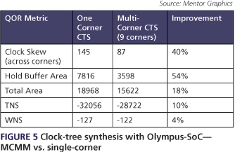
The example in Figure 5 shows how a single-corner CTS implementation compares with a nine-corner CTS implementation for a nine-corner design. Designers using MCMM CTS have achieved significant reductions in area, the number of buffers, skew, total negative slack (TNS) and worst negative slack (WNS), and dynamic power.
The other way to reduce capacitance in the clock tree is to optimize the leaf clusters. Most capacitance in clock trees is found in the pin and wire capacitance of leaf cells. CTS can provide optimization by downsizing registers and clumping them to minimize leaf wire length. However, to do this accurately, CTS must have constantly updated data about the design’s timing and parasitics. This requires a fast, incremental extraction engine and MCMM timing analysis to give accurate feedback on CTS decisions.
Last but not least, clock gating is a very common technique for lowering clock-tree power by shutting off the clock to unused sinks, preventing toggling that uses power but serves no useful function. How the clock gating is implemented varies across CTS tools. Ideally, the tools should make dynamic trade-offs between clock-gate placements based on power consumption, and enable timing constraints. As illustrated in Figure 6, if the probability of switching is equal on both sides of a clock gate, CTS should balance the tree for the best buffer count and lowest wire length. If the toggle rates on either side of a clock gate are different, CTS should minimize the wire length on the high-frequency wires to lower power, even at the expense of higher buffer count or wire length. 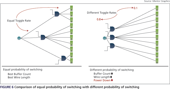
A final consideration in low-power physical design is tool capacity. Designers are often forced to implement their larger designs piecemeal, never seeing all the information they contain in context at once. This is of particular concern when optimizing for timing and power in a full-chip context, and when considering multiple corners and modes concurrently during CTS and other steps. Physical design tools should be capable of processing 100 million gates or more (hierarchical or flat), so that you can perform full chip-level optimizations without having to use ‘black box’ abstractions. In addition to providing better design results, this also greatly simplifies data management and reduces turnaround time.
Mentor Graphics
Corporate Office
8005 SW Boeckman Road
Wilsonville
OR 97070
USA
T: 1 800 547 3000
W: www.mentor.com