Overcoming the power/performance paradox in processor IP
The configurability of processor IP such as Synopsys’ ARC HS family gives designers the option to optimise for power, performance or a combination of both.
The next generation of applications demands processing performance that would be unthinkable a few years ago. Many SoC designs are using multiple processors to achieve this performance, but this comes at the price of increased power consumption. This is a problem for mobile devices with fixed battery lives, and is becoming an issue for tethered devices that have to limit the heat they generate, or which are sold on the basis of their energy efficiency.
The power/performance paradox is challenging because the typical way to deliver a higher-performance processor is to use more transistors, which increases an SoC’s power consumption and size. Many of the latest high-end processors use superscalar or multithreading schemes to achieve greater performance, but this additional complexity reduces the performance-efficiency (DMIPS/mW, DMIPS/mm2) of the cores, making them challenging to use in embedded applications. The complexity of these processors can also limit how fast they can be clocked, forcing designers to make tradeoffs to use them in higher-end designs. What is needed is a processor that delivers performance, can be clocked at GHz speeds, and uses power sparingly.
The ARC HS embedded solution
Synopsys’ ARC processor IP cores have been licensed by more than 190 companies and are used in more than 1.5 billion products a year. This has given the company deep insights into the needs of embedded SoC designers. The result is the ARC HS family of 32bit embedded processors, based on the ARCv2 architecture.
The processor family has been designed to deliver the performance needed today, with the headroom necessary for the next generation of products, and good performance efficiency.
The processors can be clocked at 2.2GHz on typical 28nm processes, delivering 4200 DMIPS per core while consuming only 80mW.
There are two members of the HS family: the HS34, which features closely coupled instruction and data memory and is designed for hard-real-time applications; and the HS36, which supports instruction and data caches and is designed for high-end embedded use. Both are available in dual- or quad-core versions, with the most powerful variant capable of delivering more than 15,000 DMIPS total performance on a 28nm process.
HS features
The HS processors are designed for use in high-end applications such as solid-state drives, connected appliances, automotive controllers, media players, digital TV, set-top boxes and home networking, and have a range of features that make them ideally suited for embedded applications. They are highly configurable so they can be optimized for each instance on an SoC to maximize performance and minimize power.
Users can also add custom instructions that tightly couple a user’s proprietary hardware accelerators to the processor, boosting performance and adding differentiation to their SoC. The processors can be configured with a second register file to enable fast interrupt and context switching without the need to save or restore core registers.
The processors have support for DSP instructions, and SIMD capabilities for signal-processing applications. The HS family also has a robust interrupt architecture supporting up to 240 independent interrupts with 16 levels of priority, as well as auto save and restore to simplify interrupt handlers.
Processor architecture
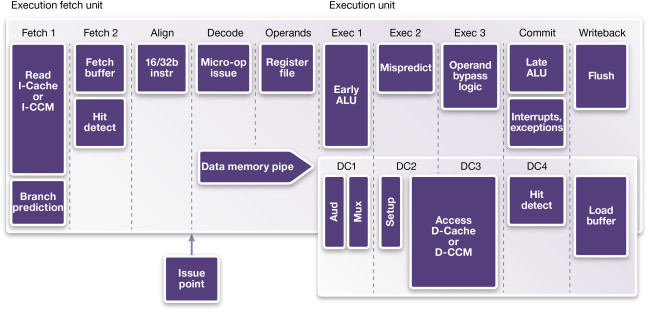
The processor family uses a power-efficient single-issue, 10-stage scalar pipeline. To improve performance, the processor supports limited out-of-order completion for long-latency instructions. Instructions graduate when they advance from commit to writeback without a result. Graduated instructions are kept in a buffer and receive a unique identification tag. The buffer can hold up to eight instructions in flight, and when their results become available they request retirement.
The HS processors have sophisticated branch prediction that offers high accuracy and early detection of mis-predicted branches. They also have an ALU in the 9th stage, which means that the processing of some instructions can be delayed from the Early ALU in the 6th stage in the case of branches or interrupts that require the pipeline to be flushed. In these cases the pipeline continues to process instructions at the back end while the front end is being reloaded. This cuts the load to use time, and for many instructions can eliminate it.
Figure 1 The ARC HS processors are built on a 10-stage pipeline (Source: Synopsys)
The HS family processors have a parallel load/store pipeline starting at the 6th stage to improve performance for data handling. They support 64bit loads and stores to and from register pairs to move data faster. They feature non-aligned load, store access that uses banked data closely coupled memory and data cache memories, enabling them to complete without extra cycle penalties. There is also an optional low-latency memory port for fast access to peripherals and memory. This port supports single-cycle access to all peripheral registers or memory on an SoC and reduces system latency by taking this traffic off the multilayer AMBA bus. The processors further improve the efficient movement of data by supporting I/O coherency with snooping of data cache, and a programmable address space that keeps the cache coherent with the shared memory of peripherals but doesn’t interfere with normal cache operations.
Configurability
There are more than 10,000 configurable options for an HS family core, encompassing almost all aspects of the processor.
The configuration capability enables HS processors to be used for many applications with substantially different functionality and interfaces on the same SoC.
In terms of performance, an HS34 can be configured down to a size that is comparable to a low-end processor but which still offers two to three times the performance.
At the block level, the processors can be configured with a variety of optional hardware, such as multiply and multiply-accumulate options. The optional radix-4 hardware divider is configurable and enables the user to trade off the number of clocks needed to complete the operation, the resulting circuit area and power consumption. There’s also an option to include a IEEE-754 compliant floating-point unit (FPU) that supports single- or double-precision operations.
At a more detailed level, for example, designers can configure in an auxiliary bus on an HS processor to enable single-cycle read/write access to all of the peripheral functions on chip, reducing system latency while improving processor performance.
The HS family support for APEX custom instructions enables users to add proprietary hardware accelerators to the processor. Users can add up to 190 custom instructions, and add up to 28 registers to the register file to act as their source and destination.
Condition and status codes can also be added and memory-mapped blocks are supported. The custom instructions can be blocking or non-blocking, and the processor supports their out-of-order completion. Custom instructions are added to an HS family processor with the ARChitect tool, which has a four-step wizard to help users add proprietary Verilog hardware to the processor.
Multi-core options
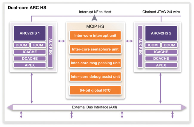
Figure 2 Dual-core ARC HS implementation (Source: Synopsys)
Dual-core and quad-core versions of the HS34 and HS36 processors are available. The multicore versions feature inter-core hardware that eases message passing, interrupt handling, semaphores and debug. The inter-core message passing uses a centralized SRAM shared by all the cores, with round-robin arbitration to manage simultaneous accesses. The inter-core interrupt capability enables each core to generate interrupts to the other cores, and each core can receive acknowledges from any other core. The inter-core semaphores are provided for synchronization across shared resources. The inter-core debugger can simultaneously or selectively halt, run, or reset any combination of the cores. The multi-core implementations also have a 64bit global real-time counter to synchronize multiple threads.
All ARC HS processors support the Synopsys STAR memory system memory test-bus interface, enabling high-quality memory test coverage and yield enhancement through memory repair. The HS family also supports ECC on all memories, and can be configured with a memory protection unit supporting up to 16 protected memory partitions.
ARC HS tools
The HS family is supported with a complete suite of development tools.
The ARChitect tool delivered with every ARC processor enables rapid processor configuration through an intuitive GUI. The output from ARChitect is Verilog RTL source, the makefiles for the nSIM and xCAM simulators, synthesis scripts for the build tools, configured setup files for the MetaWare compiler, and test benches. The output from all of the tools integrates with all the others, so the processor’s configuration and any custom instructions are recognized and used by all of the tools.
The MetaWare Development Toolkit includes an optimized C/C++ compiler, a debugger that can be used to debug real and virtual targets, and an instruction set simulator. The debugger supports debugging of up to 256 processors in a single session. It supports simultaneous debug of the dual-core and quad-core versions of the HS family. The source, disassembly, registers and variables for each processor can be viewed side by side or one at a time. The MetaWare Development Toolkit runs within an Eclipse IDE, and can be used with the SmaRT and Real-time Trace (RTT) options for real-time trace available for the ARC HS family.
The RTT option supports multiple CPUs and meets the Nexus 5001 standard. The RTT option is configurable and can use existing system storage memory, probe memory or a combination of both. There are both on-chip and off-chip capture modes. The capture elements have programmable filters and compression modules to reduce output bandwidth.
The xCAM tool supports 100% cycle-accurate simulation of the HS family processors. The tool supports the generation of an unlimited number of configurations of an ARC processor and can be used with the ARChitect and MetaWare tool. Synopsys also offers the nSIM Pro instruction-set simulator that offers ‘cycle-close’ simulation, but at very high speeds. The NCAM mode supports processor-centric algorithmic development and optimization.
Summary
The HS family of 32-bit processors has been designed to offer both performance, and performance efficiency for high-end embedded applications. Their configurability means that designers can optimize each instance of the processor on an SoC to give the maximum performance at the minimum power consumption. This combination of high performance with configurability enables designers to address the power/performance paradox and deliver their next-generation embedded designs without compromise.
Author
Mike Thompson is senior manager of product marketing for ARC processors at Synopsys.

