Moving to advanced reliability verification
Shrinking process nodes, rising power efficiency goals and burgeoning device functionality are stretching existing DFR techniques to their limits. This scalable methodology looks to address the shortfall.
Relentlessly shrinking process nodes and the need to balance increasing functionality with greater power efficiency highlight the importance of reliability verification. On one hand, devices and conductors are shrinking, device oxide layers are getting thinner, and the number of power domains is rapidly increasing. On the other – and for reliability in particular – there has been a dramatic increase in digital content for sensitive applications in the automotive, medical, and communications markets. The article describes these tensions, and a new scalable methodology that addresses the shortfall of existing techniques. As failure becomes as much about time-dependent as ‘sudden’ breaks, how can engineers adapt to the challenges ahead.
More reliability issues
Reliability used to be bought with a little over-engineering and some additional real estate. It was verified by eyeballing the layout to determine which structures might cause reliability problems. You would visually inspect structures on PADs and examine the exterior to make sure all were correctly configured. After, you would tweak the design as appropriate.
This does not work anymore. Designs are too big and complex; manual methods are too unreliable. In addition, designers must optimize for performance, area, and reliability within explicit, hard-earned margins.
Moreover, where the emphasis used to be on preventing catastrophic failure caused by external factors, designers must now address more subtle degradation mechanisms.
The growing list of design for reliability (DFR) issues confronting designers includes:
- Time-dependent dielectric breakdown (TDDB)
- Negative bias temperature instability (NBTI)
- Hot carrier injection (HCI)
- Threshold voltage shift (Vt)
- Electromigration (EM)
- Electrical overstress (EOS)
- Latch-up
Rather than causing hard failures (which happen quickly and are quite obvious), many of these happen over time. They are often difficult to predict, and once a product gets a reputation as unreliable, it can be very hard to overcome that even if the problem is fixed.
The industry is looking more closely at IC reliability issues. The ESD Association has been working on a technical report1 that focuses on electrostatic discharge (ESD) checking and how best to address typical ESD issues during design. The Reliability Simulation Council is researching ways to improve reliability in IC design.
Outsourcing has added another wrinkle. Not just moving to a smaller node but moving to another or second-sourcing from a different foundry can disrupt the effectiveness of ad hoc approaches.
It is clear that access to a well-defined set of reliability best practices is crucial to maintaining productivity and forward momentum.
Traditional approaches
Marker layers
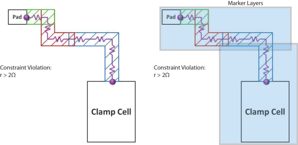
A conventional design rule checking (DRC) tool requires the designer to identify the physical locations where reliability checks should be applied. This is done by adding extra virtual layers (‘marker layers’) to the layout database. These do not represent actual transistors or wires, but regions that trigger specific checks to verify proper DFR practices (e.g., making sure a wire is extra-wide, or that some wires have different spacing where there are greater voltage potentials).
Figure 1
Point-to-point resistance checks in ESD protection circuits with applied marker layers (Source: Mentor Graphics – click image to enlarge)
Marker layers are created manually and the process is both tedious and error-prone. The layers require additional DRC runs that add to design cycle time. Also, they are hard to maintain following design revisions or when the designer who has created them moves to another project (this is particularly true given today’s increasingly large design teams). Marker layers cannot provide the level of confidence required today.
SPICE simulation
Some reliability checks require knowledge of the voltages present at each node in the circuit. For example, checking that the voltage between gate and source or drain does not exceed the breakdown voltage of the gate’s thin oxide can be challenging in a multi-voltage domain design. The traditional strategy is to use a SPICE simulation that provides voltages and currents at each node over time as the circuit is driven by a set of vectors that enables simulation for all the expected modes of operation. Unfortunately, such simulations are extremely time-consuming in terms of setup and run time. In addition, there is the time needed to evaluate results: significant insight is needed to properly interpret the resulting waveforms.
Moving to a scalable solution
Designers need a robust, scalable strategy that captures and enforces best practices across large teams as the technologies they use evolve. This section describes such an approach that extends conventional physical verification technology to not just realize but also automate the delivery of these goals.
A scalable reliability verification solution must:
- characterize the physical system and verify it against a well-defined set of best practices or rules;
- avoid full simulations where possible to save time and computing resources; and
- allow engineers with general expertise to verify designs against highly specialized reliability design requirements.
A scalable IC reliability tool therefore has to include key functionality not traditionally associated with physical verification. Specifically, it must:
- support topology recognition using netlist criteria to identify physical structures of interest;
- support propagation/connectivity rules to establish specific relationships between identified structures of interest;
- evaluate physical rules applied to the results of the first two processes (the conventional function of layout verification tools); and
- integrate with the normal PV flow.
In a sense, the key challenge in reliability checking lies in bridging the gap between the logical and physical views of the design. Logic and analog designers think in terms of schematics and Verilog descriptions. Physical (layout) designers think in terms of geometries, widths, lengths, and feature spacings. Tools for their particular disciplines have evolved along the same lines. Reliability checking requires a combination of these views, a challenge for both the tool developers and the engineers who use those tools.
As noted, a major problem for many reliability plans lies in identifying exactly where in the layout the checks should be made. Without a way of narrowing their scope, check runs will generate an overwhelming number of false positives on most designs.
Consider a rule to detect incorrect supply voltage connections in a multi-voltage domain, low power SoC. Simply specifying that a transistor can only be connected to one domain will generate false positives for all the level shifters and isolation gates.
We have seen the limitations in techniques such as marker layers, which operate only on the physical view. A better approach would allow us to specify the areas of interest in the logical domain in terms of the netlist, while performing required physical measurements on the layout.
As well as topology recognition, we need a way to trace logical and physical relationships. For example, to detect violations of gate breakdown voltage limits due to incorrect voltage domain crossings, we must be able to propagate supply voltages to all the nodes in the design. And we want to do this in a static mode to avoid time-consuming simulations. Once we propagate the voltages, we can use topology recognition to eliminate structures that intentionally have multiple domain connections, such as level shifter circuits. This resolves the false positives issue and delivers fast and efficient results.
Performing a TDDB check
To demonstrate how designers can use new reliability verification tools that combine topological and physical layout information, this section describes an example check based on Calibre PERC from Mentor Graphics.
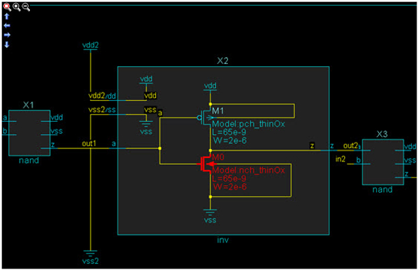
Figure 2 shows a circuit containing PMOS and NMOS thin-oxide gates with direct and indirect connections to power the domains VDD2 and VSS2. An indirect connection may be made through another transistor, diode, resistor, or some other circuit element. These connections often form the basis of ‘missed’ paths that are not readily identified during design reviews, particularly when the indirect path is through a circuit elsewhere in the design hierarchy that is not obvious. The local power connections in the sub-circuit itself (VDD/VSS) are seen in the context of the larger design. The external connections to an otherwise-verified IP block must be evaluated.
Figure 2
Checking thin-oxide gates with direct and indirect paths to VDD2/VSS2 (Source: Mentor Graphics – click image to enlarge)
To identify the thin-oxide gates at risk, a designer must define a check (expressed here in pseudocode for simplicity):
- Identify power domains in the design.
- Identify which power domains are ‘not safe’ for thin-oxide gates.
- Identify the specific device types and subtypes that corresponding to thin oxide MOS devices.
- Check the related ‘source’, ‘drain’ or ‘bulk’ pin connections on these thin-oxide MOS devices to power domains.
- Evaluate both direct and indirect paths.
- Flag an error for thin-oxide MOS connections to ‘not safe’ power domains.
Complex systems often have multiple power domains that require complex design rules to determine which domains are safe and under what conditions.
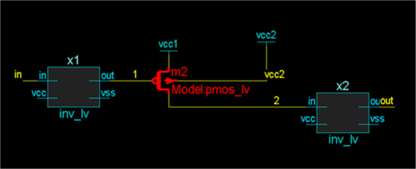
Verification of bulk pin connectivity is particularly important in determining whether a circuit is susceptible to these time-related reliability issues. As shown in Figure 3, an incorrect bulk connection may make this PMOS gate vulnerable to NBTI attributable to a higher bulk voltage.
Figure 3
A thin-oxide PMOS (Model: pmos_lv) with a path to high voltage may lead to NBTI susceptibility (Source: Mentor Graphics – click image to enlarge)
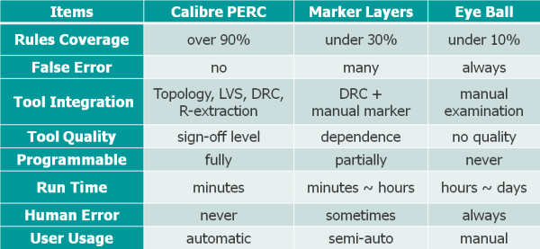
When compared to existing reliability techniques, it is clear that those offered by automated reliability verification tools such as Calibre PERC are necessary to ensure today’s designs can not only be manufactured, but will also perform to specification throughout their intended lifecycle (Table 1).
Table 1
Point-to-point resistance checks in ESD protection circuits with applied marker layers (Source: Mentor Graphics – click image to enlarge)
Adopting the new technology
Because it requires design and verification engineers to change the way they think, project managers need to move carefully and thoughtfully in adopting this technology. There are two primary strategies available: top-down and bottom-up.
Where there is already a centralized process in place to document, maintain and improve reliability practices, typically under the auspices of a CAD or QA organization, it will probably make sense for this group to initially implement new reliability checks in the tool for others to use. This top-down strategy disseminates configured tools to the IC design and verification communities.
A bottom-up approach will usually emerge from a small group of individuals who identify better ways to improve the efficiency and effectiveness of verification tasks. As they use any new tools, word of their better efficiency and results will get out, resulting in a groundswell of requests for the same technology. At some point, support for these requests can be transferred to the CAD organization to alleviate the local support burden and provide a uniform experience across the company.
Conclusion
IC reliability verification is hard. To get it right, you need to give it explicit attention and employ the most effective tools at your disposal. But it is no longer just icing on the cake. IC reliability is rapidly becoming a make-or-break competency for creating successful IC products capable of delivering long-term reliability.
References
1. EDA Tool Working Group, ESD Electronic Design Automation Checks, ESD TR18.0-01-11, 2011
Links
ESD Association: http://www.esda.org/
Reliability Simulation Council: http://www.linkedin.com/groups/Reliability-Simulation-Council-4220058/about
Author
Matthew Hogan is a Calibre marketing engineer for Mentor Graphics. With over 15 years of design and field experience, he is well-versed in today’s aggressive design issues. Matt is an IEEE senior member and ACM member. He holds a B.Eng from the Royal Melbourne Institute of Technology and an MBA from Marylhurst University. Matt can be reached at matthew_hogan@mentor.com.


