A holistic approach to IoT chip design
Many Internet of Things (IoT) applications share two key design constraints: they need to be small and they need to consume as little energy as possible. The most effective way to address these challenges is to take a holistic approach, co-optimising the choice of circuit architectures, design styles, tools, IP and processes.
IoT SoC architectures
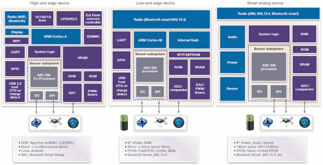
There are three common SoC architectures for IoT devices: application processors (high-end), microcontrollers (low-end), and smart analog (see Figure 1).
Figure 1 Alternative architectures for IoT devices (Source: Synopsys)
High-end edge applications borrow from mobile phone and tablet architectures, and usually include processor cores with MMUs, external DRAM, LCD controllers and GPUs. They tend to use Android or Linux and provide software developers plenty of memory. They’re currently built on 28nm processes.
Low-end edge applications are usually microcontroller-based, with embedded flash or lower-cost and more power-efficient non-volatile memory (NVM). The resultant SoCs often run a real-time operating system, and may include wireless connectivity. This is made possible by 90nm mixed-signal processes, some of which also have embedded Flash or NVM options.
Adding smarts to analog devices such as sensors and power management ICs has traditionally required an external microcontroller. However, it is becoming more common to integrate such cores, and NVM with power management and MEMs sensors on a die to enable software programmability, typically on 180nm processes. This will reduce system costs and optimize the supply chain compared to building a PCB with multiple devices.
Powering the Internet of Things
Energy efficiency will be at the heart of the IoT design challenge for years to come. Some IoT devices will always be on and so reducing dynamic power will be critical; others will be asleep for 99% of the time, so designers will need to minimize static power.
What can the semiconductor community do to help? Some foundry processes are being adapted to run at lower leakage and voltages. Designers are borrowing techniques such as clock and power gating, multi-voltage domains, DVFS and back-biasing from the mobile market. IoT teams are also applying smart biasing, sub-threshold and near-threshold design techniques and making more aggressive use of power management strategies. Tools vendors are developing supporting techniques, such as tools that ensure the consistent interpretation of power intent; effective power network synthesis; optimal low-Vt usage; and comprehensive power-aware formal and static verification.
IoT-specific IP
The largest opportunity for the semiconductor community to contribute is by providing IP that is optimized for power while providing just enough functionality to get the task done.
IP in the form of logic libraries, memory IP and compilers will need to be optimized beyond current mobile IP, including always-on thick-oxide solutions, low voltage operation, multi-channel length transistors, multi-bit flip flops, integrated test and repair with embedded flash and ultra-low power NVM IP, as a few examples.
Processor cores and subsystems will also have to adapt to the IoT. One method to cut power consumption would be to use highly optimized cores which can do more, quicker, using very fewer memory resources, to reduce the energy cost of running a core for a long time and multiple memory accesses. Optimized co-processors, for example for sensor fusion, power management, motor control, voice, vision, and others specific functions will also save energy.
Application-specific analog interfaces can also be used to manage features such as metering, medical and power management to better control a system and so increase its energy efficiency.
IoT design teams are already making the most of low-power interfaces designed for mobile and networking markets, such as low-power DDR, MIPI for camera and display, Ethernet, and USB.
To cut peak currents and task time, designers are implementing new wake-up features, waking up from lower power NVM or ROMs, using more flexible sleep modes and integrating interoperable low-bandwidth wireless radios such as Bluetooth Smart.
Saving energy
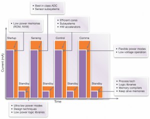
Here are some techniques for cutting energy use during common phases of an IoT design’s operation (see figure 2):
- Boot from ROM or low-power MTP NVM options rather than embedded flash, or slow the memory loads during start-up to reduce peak currents.
- Develop a more granular approach to power management, so that there are optimized low-power modes for use after start-up but before initial sensing and measurement calculations begin.
- Use of processor cores and architectures that enable significant reductions in cycles and wait states during sensing and measurement. This, coupled with higher speed and lower power data acquisition, improves system control and saves energy.
- Process complex algorithms at minimum frequencies by using more efficient processors to reduce system power usage as well as system mechanical and PCB costs. For example, the use of vector-based techniques has improved motor control over the past few decades, enabling the use of smaller motors.
- Ensure applications communicate at the right time and with the right amount of data to optimize their energy usage while shutting down unnecessary components when not in use.
- Keep devices in the right sleep states, only powering the ‘always-on’ circuits. Minimize leakage with optimized IP and a low-power design methodology.
Figure 2 Common techniques for saving energy in IoT designs (Source: Synopsys)
Summary
IoT designers face other challenges apart from energy management, such as the pressure to increase integration, cut system costs, add connectivity and security, and simplify their supply chains. They need to achieve these goals while improving ease of use, meeting aggressive project schedules and getting to market first.
IoT is a fast-moving, fragmented market spawning hundreds of companies, applications and products. Teams that use IP tailored to address specific IoT challenges, as part of a holistic approach, should get their designs done more quickly and at lower risk than otherwise. This is particularly important as companies compete to establish their devices and ecosystem as the standard for their sector of the IoT market.
Further information
Author
Ron Lowman is the strategic marketing manager for IoT at Synopsys. Prior to joining Synopsys, Lowman spent 16 years at Freescale, most recently as industrial business development manager for Freescale’s microcontroller division and product marketing manager for industrial MCUs and digital signal controllers. Lowman has also held several product management and marketing roles, strategic technology and business operations roles, and engineering roles including automotive product and test engineer, factory automation controls engineer, and foundry process engineer. Ron holds a Bachelors of Science in electrical engineering from The Colorado School of Mines and a Masters in business administration from the University of Texas in Austin.


