Clock-domain and reset verification in the low-power design era
The multiple clock domains on today’s SoCs create a hotbed for clock-domain crossing bugs to thrive. Low-power design techniques increase the complexity of tracking these bugs down. Find out how these failures arise and what to do about them.
SoCs integrate components from many sources. Accompanying this abundance of features is significant complexity that needs to be correctly handled. One source of complexity is that multiple components may operate at very different clock frequency ranges from their counterparts. Further, the clock inputs into many logic cones will be selectively disabled to save energy.
The existence of multiple clock domains, the need for signals to cross between them, and the use of clock-disabling logic to save power create a hotbed in which clock-domain crossing (CDC) bugs thrive.
CDC bugs lurk at the crossroads of bad design implementation, overlooked timing paths and incomplete verification. If the signal crossing from one asynchronous domain to another arrives too close to the receiving clock edge, the captured value can be non-deterministic due to setup or hold-time violations. This ‘metastable state’ results in incorrect values being propagated downstream, causing functional errors. The failure signatures are unpredictable and intermittent making them hard to detect and diagnose via simulation or in the lab.
Figure 1 A nondeterministic value is captured if a signal passing between clock domains arrives too close to the receiver's clock edge
Many clock domains creating thousands of crossings significantly increases the verification effort. The subtlety of CDC issues and that volume of crossings often lead to CDC bugs slipping through to tapeout. They frequently result in failures in the field requiring re-spins and incur costs in the millions of dollars.
Traditional clock and reset mechanisms were based on a master scheme distributed throughout the chip. Today’s die size is so large that this has become impractical. Also, power management requires that multiple power and clock domains on the chip can be turned on and off independently.
Clock frequencies in communicating domains (asynchronous or not) can differ by an order of magnitude and vary dynamically based on throughput or power optimization requirements. The proliferation of gated clocks for power optimization has added tools to the design flow, automating the addition of clock gates previously undertaken by logic designers.
Clock gating
The premise for gated clocks is that there is no modification to the original functionality. Logical equivalence checking (LEC) tools are employed to ensure this is the case.
The number and variety of clock-gating techniques, the nontrivial control circuitry involved, and the likelihood that most will be automatically inserted will complicate verification. The implementation of power-up reset is also more complex today as it optimizes for both power and physical layout.
Clock and reset schemes must be comprehensively verified before you analyze the rest of the design. Many issues initially diagnosed as control or datapath-related are eventually traced to improper clock and reset behavior.
The fact that synthesis and power optimization tools are not glitch-aware exacerbates the problem. There is a distinct possibility that glitch-susceptible logic will be inserted during optimization. So, verification tools for clock and reset analysis should operate at both the RTL and the gate level.
Several techniques are used for clock gating[1]. The first, combinational clock gating, is a relatively straightforward way of disabling the clock to registers when their output does not change. It involves identifying combinational logic conditions that cause a register to hold its previous value and using them as an enable signal for the clock pin instead.
Figure 2 Combinational clock gating
Opportunities to insert combinational clock gating can be identified by power-aware RTL synthesis tools based on an analysis of the combinational cone of logic between registers. Once insertion is complete, LEC ensures that the result is functionally equivalent to the original. The synthesis tool however is not CDC-aware. It might perform optimizations that violate CDC principles at the boundary interfaces between domains.
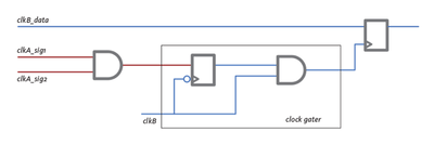
Figure 3 Potential glitch on clock path due to an asynchronous enable signal
In Figure 3, two clocks (clkA and clkB) are asynchronous but control signals that feed into a single logic path. The synthesis tool may infer a clock gater in domain clkB for a flop that captures data from clkA. To optimize for power, the tool derives the enable for the clock gater using a combination of signals from clkA.
Due to the asynchronous nature of the enable, there could be metastability at the clock-crossing boundary. This would lead to non-deterministic behavior in the clock-gating logic, resulting in intermittent data loss or corruption – a notorious source of ECOs. LEC will not catch this problem. Specific steps are needed to identify and eliminate such issues.
A second technique, sequential clock gating is more complicated. It identifies enable signals based on an analysis spanning multiple clock cycles. By examining the design across sequential boundaries, advanced power optimization tools identify data dependencies, observable ‘don’t-care’ conditions and unused states. They then formulate enable conditions to shut down the clock to groups of flip-flops. Sequential gating provides greater power savings compared to its combinational counterpart as it can turn off more registers for more clock cycles.
A practical implementation of a sequential scheme is to turn off subsequent banks of pipeline registers based on the propagated value of the enable signal in the current pipeline stage. This can be boiled down and restricted to a single flop.
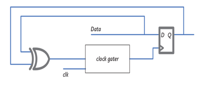
Figure 4 XOR self-gating
A third technique is XOR self-gating. It is possible to gate the clock to a flop based on the output of the flop in the previous cycle and the incoming data value. A simple XOR of the output and incoming input can be used as the enable signal for the gater (Figure 4). Power optimization tools use this technique.[2]
Recall the combinational example where a synthesis tool inferred clock-gating logic susceptible to metastability. A similar situation can arise during power optimization. In Figure 5 a control signal is properly synchronized with a dual-flop synchronizer. An automated power optimization tool that is not CDC-aware might not recognize the synchronization mechanism and insert gaters on individual flops of the synchronizer.
Figure 5 XOR self-gating transformation
CDC guidelines dictate that the output of the first flop of a synchronizer is susceptible to metastability and should not be used functionally. The transformation introduced by the power optimization tool violates this dictum by using the output of the first flop of the synchronizer to derive the enabling condition for the clock gater. This can cause non-deterministic operation of the gater, leading to spurious control signal values propagating downstream and functional control flow failures. Again, LEC tools will not catch such issues.
Real Intent’s Meridian CDC tool runs a suite of checks on clocks, derived clocks and gated clocks. It pinpoints issues such as glitches, unsafe CDC practices, non-deterministic clock states and incorrect gating. It protects against unintentional yet catastrophic side-effects attributable to synthesis and power optimization tools.
CDC issues can occur when an asynchronous reset control crosses clock domains but is not synchronously de-asserted. This can cause a glitch in control lines to a finite state machine.
This scenario is at the confluence of three design requirements, and results in a failure if one is not met:
A. The need for multiple clock domains that can be independently reset.
B. The need to use flip-flops that are asynchronously reset.
C. The need for reset signals to be asynchronously asserted but synchronously de-asserted.
Let us delve into each in more detail.
A. Multiple clock domains that can be independently reset.
After a failure, a hardware reset restores the system to a known state from which it can start functioning deterministically. Power-cycling a modem is a classic example of allowing enough time for a reset to propagate to all subsystems, some of which might have different clock frequencies. From a verification viewpoint, as these subsystems are designed and verified separately, the presence of a reset in each enables effective block-level verification by ensuring that the design is in a known state for simulation.
It is good practice for every flip-flop in a design to be resettable. To extract higher performance in functional mode there may be certain parts, that are not resettable but whose upstream registers are (e.g., the pipeline registers). In such cases, the design takes more clock cycles to enter a known state as the upstream reset values need to propagate down to these registers. Often, this is an acceptable tradeoff but one that designers must consider carefully when determining reset strategies.
Several benefits stem from the ability to independently reset subsystems. These include:
1. Managing functional complexity of the system.
2. Avoiding long latency on a system reset after a subsystem failure.
3. Being able to run simulations on a subsystem level before integration.
B. Flip-flops that are asynchronously reset.
Having established the value of multiple resettable clock domains, the question arises of which type of reset to use.
By definition, a synchronous reset is one where the reset occurs during the active edge of the clock feeding the flip-flop. Since the reset signal is timed, the flip-flop is immune to glitches occurring away from the active clock edge. Such glitches that occur on the reset line or in combinational logic feeding the synchronous reset do not affect the flip-flop as the reset is only sampled at the clock edge.
However, the requirement that a synchronous reset has an active clock is double-edged. As noted, SoCs are being architected to reduce power consumption. One way this is achieved is by turning off clock and power domains when unused.
Turning off the clock to a subsystem violates the premise on which synchronous reset is based: That the clock to the flip-flop being reset be active. Only an asynchronous reset will work. It does not require the presence of an active clock edge during reset assertion.
Asynchronous resets are incorporated into flip-flops via a reset pin and do not need an active edge of the clock for reset assertion. If the polarity of the reset signal is active-low, the flip-flop gets the reset value when the reset signal is de-asserted.
Unlike synchronous resets, asynchronous resets are not involved in the logic feeding the ‘D’ pin and hence do not factor into the single-cycle timing of the datapath. This lets designers tune the datapath without worrying about delays from the reset-related logic.
A system with multiple clock domains requires the use of asynchronously reset flip-flops to:
1. Have the ability to reset flip-flops to a known value; and
2. Be able to do so without the clock to those domains being active.
C. Reset signals that are asynchronously asserted and synchronously de-asserted.
The use of asynchronous resets may mean you can reset a subsystem without an active clock edge, but there is a catch. They are, by definition, asynchronous during both assertion and de-assertion of reset. The assertion, as discussed, does not pose an issue as it is independent of the clock signal. However, the de-assertion must meet reset recovery times. The reset recovery time is similar to a setup timing condition on a flip-flop; it defines the minimum time between the de-assertion of reset and the next active clock edge.
If the asynchronous reset is de-asserted near the active edge and violates the reset recovery time, it could cause the flip-flop to go metastable, resulting in the potential loss of its reset value. A non-deterministic reset value defeats the purpose of using a resettable flip-flop. Hence, a fully asynchronous reset is not a viable solution for systems with multiple clock domains.
If synchronous resets have issues during reset assertion and asynchronous resets have them during reset de-assertion, overcome them by using the best of both worlds: A scheme that involves asynchronous assertion yet synchronous de-assertion.[3]
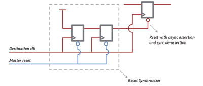
Figure 6 Reset synchronizer
With a reset synchronizer, (Figure 6), the main reset signal entering the subsystem asynchronously resets the two flip-flops forming the reset synchronizer. This synchronizer then drives the signal for the rest of the subsystem ensuring that all the flip-flops in it are asynchronously reset. This reset assertion is asynchronous to the subsystem clock, which need not be active at the time of reset. When the main reset signal de-asserts, it takes two active clock edges for the subsystem flip-flops to be taken out of reset. Since this reset removal is governed by the active clock edge, the de-assertion is synchronous.
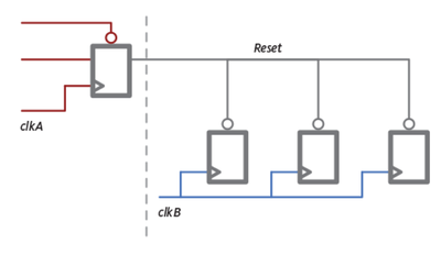
This use of reset synchronizers is a robust and reliable solution for reset distribution. Meridian CDC identifies situations where such schemes can protect against subtle metastability issues in the reset architecture. In Figure 7, the flip-flops in domain B would be identified by Meridian CDC as being asynchronously reset from domain A without the use of a reset synchronizer.
Figure 7 A CDC tool should be able to identify that domain B is reset asynchronously from domain A
Traditional CDC verification using linting, template-based approaches, hacked simulation or static timing does not scale to meet the challenges posed by today’s SoCs. There is an immediate need for a solid CDC verification tool with a robust methodology that integrates well with existing tool flows and is flexible enough to accommodate new power optimization flows without compromising coverage.
Vaishnav Gorur is senior applications engineer at Real Intent
References
[1] Utilizing Clock-Gating Efficiency to Reduce Power, Mitch Dale, Calypto Design Systems, EE Times, Jan. 2008
[2]Reducing Power with Advanced Synthesis, Technology Update, Synopsys
[3] Asynchronous and Synchronous Reset Design Techniques – Part Deux,
Cliff Cummings, Don Mills, Steve Golson, SNUG 2003
Contact
Real Intent, Inc
990 Almanor Avenue
Suite 220 Sunnyvale
CA 94085
T: +1 (408) 830-0700
W: realintent.com


