Using advanced planarity analysis to drive smarter filling strategies
Designers have been using dummy fill to address design for manufacturing for some time, but the process of simply wallpapering shapes into a design’s “white space” to help it maintain planarity can no longer cope with the complex challenges presented at today’s advanced process nodes. Not only is planarity harder to maintain, but there are other manufacturing and electrical issues that arise and, taken together, all these factors demand more thorough analysis of the potential impact of any fill strategy, be it undertaken on either a bottom-up or top-down basis. The article reviews the latest challenges and emerging techniques for addressing them, with some suggestions as to how engineers might approach the implied shift to “smart fill”.
IC designers are familiar with the technique of metal filling to improve the planarity of wafers and die as they proceed through manufacturing. In fact, filling is no longer an option—it is a requirement. Furthermore, it is increasingly important for designers to take an active role in the filling process because it impacts the parasitic capacitance of a design. The process addresses multiple manufacturing and electrical challenges on multiple layers and uses multiple methodologies. The most common reasons for fill at the metal layers, including planarity, are for etch and lithography.
Chemical-mechanical planarization (CMP) is a type of high-precision smoothing that attempts to bring the wafer back to planarity after the various processing steps. Different materials (e.g., polysilicon, copper, oxide) respond to the CMP process differently, so areas with concentrations of one material can have unwanted ridges or depressions.
Another problem involves etching, (i.e., removing a material in areas defined by a photo-sensitive resist coating using a reactive ionized plasma). Variations in the amount of resist-treated versus non-treated areas within localized regions of the die cause variations in the amount of the chemical reaction that occurs in the plasma. This leads to variations in the etch rate of the material being removed, which affects the height and/or the width of the metal lines.
Improvements in CMP planarity and etch uniformity also improve the lithographic depth-of-focus (DOF) margin. The process of depositing and etching materials results in unevenness, or ‘topology’ on the surface of the die every time a new layer is added. The unevenness of previous layers and the irregularities in a current layer can cause patterns to be in different points in the lithographic focal plane. This limits the window for focal variation in any tool being used. The way to mitigate the challenges associated with planarity, etch and DOF is to use an analysis-driven fill solution.
When dummy fill is not enough
Traditionally, these issues have been addressed in the metal layers (the layers of etched copper wires that form the interconnections among the transistor switches). Designers have filled in blank areas there that do not require wires with dummy fill (Figure 1), a term that turns out to be a double entendre although it was not originally intended that way.
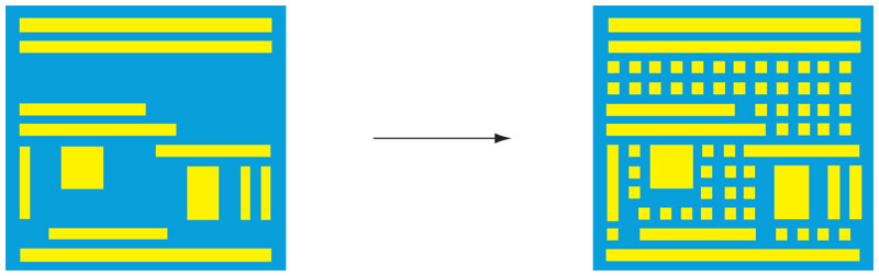
Figure 1
Dummy fill is the addition of non-functional shapes to the layout to maintain a constant density of material in each layer
The purpose of this type of fill is to smooth out the density of metal across the die and thereby reduce the inherent CMP and etch problems. The word ‘dummy’ refers to the fact that the added fill shapes (small areas of copper) serve no electrical or interconnection purpose; they exist only to balance the density of copper across the die.
The second meaning takes increasing importance as we encounter new manufacturing challenges at advanced process nodes. The traditional dummy fill algorithm was pretty dumb—just fill any white space (i.e., those areas where there are no interconnect wires) with regular shapes until they are all filled. However, at 65nm and below, many second-order effects become significant and this simple algorithm cannot deliver sufficient planarity. Designers need powerful tools to help them analyze the IC design and determine the optimum fill to satisfy planarity requirements without causing unwanted side effects.
Smart fill
The complexity of fill at advanced nodes sets some new tool requirements. The most fundamental is an ability to perform a sophisticated analysis of layout shapes across multiple layers independent of the actual filling operation. Instead of simply filling white space by looking at open areas in isolation, a ‘smart fill’ tool must analyze the design across a user-determined number of layers. Once that analysis is complete, such a tool can use the data gathered to determine the amount and pattern for the fill to achieve the user-supplied constraints.
Newer technologies have multiple constraints to optimize fill. Designers need to be able to measure a range of parameters and adjust fill to solve all those new constraints, such as:
- density range—limits on the delta between the minimum and maximum density regions;
- density gradient—specification of intra- and inter-layer density uniformity (i.e., density differences measured between adjacent areas, or ‘windows’, set by the user);
- locality effect—very local fill rules (e.g., the maximum area with no fill within a gradient window);
- layer interaction—spacing rules such as ‘fill to fill’, ‘fill to layer’ and ‘fill to other layers’; and
- priority across layers—definitions as to which constraints take precedence when filling overlapping real estate for several layers at the same time.
As these parameters imply, smart fill tools analyze the interactions among multiple windows and layers simultaneously, and then provide fill instructions for overlapping fill areas on multiple layers as a related group. The priority parameter tells the fill algorithm which constraints take precedence in cases where applying all rules at the same time would create a conflict. In a fully integrated tool, all this is done concurrently and is transparent to the user once the rules and constraints are determined. It is a very efficient and accurate way of adding fill to any design.
Advanced planarity fill
The most advanced process nodes are even more demanding. Beyond the planarity, etch and DOF issues that impact the metal layers, designers are seeing increasing demand for analysis-based filling tools for the base layers. In addition to traditional manufacturing concerns, new factors such as rapid thermal annealing (RTA) and stress are affecting the electrical behavior of a design.
RTA occurs during the annealing process step when a lamp is used to heat the wafer. This technique is sensitive to both the density and the uniformity of the pattern because it changes the local reflectivity of the wafer and hence the local temperature. This changes the final doping distribution in each area causing variations in transistor performance.
Stress that affects the threshold voltage through mobility tuning is also impacted by the density and placement of nearby shapes.
These challenges require a solution that will select the correct layer and location of the fill shapes. The key is the analysis that will drive the design rules and constraints used to select the layers and the location of the fill elements, including the placement of multi-layer fill shapes.
Selecting a flow for your design goals
Designers also have to think about the way fill is incorporated into their design. You can take either a top-down or bottom-up approach (Figure 2, p. 17).
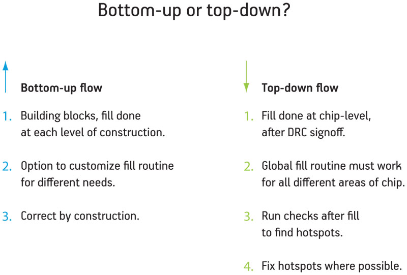
Figure 2
Both top-down and bottom-up fill strategies have their own limits and advantages
If you take a top-down approach, filling is performed at the full-chip level after DRC signoff. The layouts for all blocks are frozen and a smart fill tool applies fill to the entire design at all layers. The advantage of this approach is that the tool considers the interactions among blocks in their actual context in the design.
With a bottom-up approach, you add fill as you construct individual blocks. The fill criteria (e.g., min/max density and min/max density gradient) become part of the signoff for each block. The disadvantage of this approach is that you must understand the context in which the block will be used as the design is built. The advantage is that you can customize the fill rules for the needs of the specific block (e.g., to reduce parasitics for a timing-sensitive block). The result is a ‘correct by construction’ design that considers planarity effects throughout. The only fill added at the end of the process is between the blocks.
Some tools support a hybrid approach. They fill in a bottom-up manner, but offer the ability to define a context for the blocks as they are constructed. The user can specify a surrounding density for each block that represents the expected context into which the block will be placed. AMD has worked with the Calibre team at Mentor Graphics to add this functionality to the SmartFill function in its YieldEnhancer product. This allows the fill algorithm to consider an expected density so the gradient rules can be addressed when adding fill to the individual blocks.
A hypothetical example
To illustrate how Calibre’s SmartFill process works for the base layers, consider the design depicted in Figure 3. It shows traditional dummy fill on the upper left and multi-layer SmartFill on the lower right. As the annotation indicates, when filling the base layers, up to five layers must be added. However, which layers and how much of each layer to add is based on the analysis of three layers as a group.
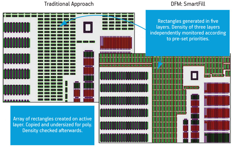
Figure 3
Dummy fill contrasted with Calibre YieldEnhancer’s SmartFill
The key to meeting our exacting design constraints is a strategy that combines the analysis of the individual layers and then sets the constraints for the filling engine. In addition, the multi-layer fill capability allows all these steps to occur in a single-pass operation. In the case shown in Figure 4, the basic fill component is made up of shapes on multiple layers:
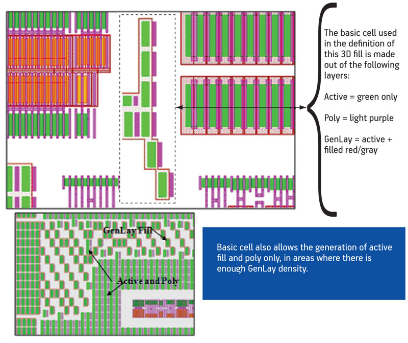
Figure 4
Using a smart fill tool, designers can define a complex fill pattern and the priorities for rules that determine how fill cells will be generated
- an active layer (green);
- a poly layer shown (purple); and
- a GenLay, a composite of two layers in which the relative shape of the two layers is maintained in a constant relationship (dotted area).
The rules for the fill process are shown in Table 1. Notice the priority column, which indicates that the rules and constraints for the poly layer should be applied first, followed by the GenLay, and, finally, the active layer. The other columns in the table specify an allowable density range, a density target, and the dimension of the window size for measurements, essentially setting the size of the context or locality over which interactions will be considered. Once these rules and parameters are set, the smart fill tool can perform the analysis and generate the fill in the optimum manner given the constraints, priorities and fill-shape definitions.
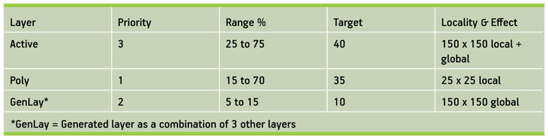
Table 1
Setting SmartFill constraints
Conclusion
Like virtually every aspect of physical design, the challenge of maintaining planarity using fill strategies is much more complex at advanced nodes. However, the requirements for a smart fill solution have expanded beyond just planarity to include both manufacturing and electrical factors. Fortunately, the tools available to designers to manage the fill process have evolved to help manage this complexity so designers can optimize their designs without adding unacceptable delay to their design cycle. AMD has investigated the use of SmartFill functions in Calibre YieldEnhancer for analyzing complex layouts and adding optimized fill, including multi-layer fill shapes. It has found such capabilities can help meet the performance and manufacturing requirements of AMD’s most advanced ICs.
Norma Rodriguez is a senior member of the Technical Staff at AMD.
AMD
One AMD Place
P.O. Box 3453
Sunnyvale
CA 94088
USA
T: +1 408 749 4000
W: www.amd.com