Computational scaling: implications for design
The article presents the context for the use of computation scaling (CS) to eke out more from existing lithography tools until next-generation techniques are finally introduced. It discusses the critical elements in the CS ecosystem developed by IBM and partners to overcome roadblocks to optical scaling that demand the use of non-traditional techniques for the incoming 22nm process node.
The differing roles of engineers in the design and process segments of a project flow are discussed, as are some of the tools that will make CS a reality.
In these early years of the 21st century, major obstacles to circuit design can be seen in terms of premature perturbations to design practices attributable to the later-than-desired realizations of advanced semiconductor technologies. The perturbations were inevitable, but they still underlined the absence of key elements from the technology roadmap. The most widely known example of this is the demise of traditional CMOS performance scaling experienced during the first half of the decade. The inability to control off current as device channel length was scaled for performance led to the architectural shift from single to multiple core processors. Although the laws of physics were unavoidable, the change in design practice took place earlier than anticipated because industry initially lacked a high-K gate dielectric material.
As we near the end of this decade, we face a similar perturbation in circuit design techniques as they relate to density scaling. Historically, density scaling has relied on lithographic scaling. However, delays to next-generation lithography (NGL) now present us with a discontinuity in the lithographic roadmap supporting that link.
IBM recognized the need for innovation to address this problem some time ago and recently announced that it is pursuing a Computational Scaling (CS) strategy for semiconductor density scaling [1]. This strategy is an ecosystem that includes the following components, alongside necessary technology partnerships:
- a new resolution enhancement technique (RET) that uses source-mask optimization (SMO);
- virtual silicon processing with TCAD;
- predictive process modeling;
- design rule generation;
- design tooling;
- design enablement;
- pixilated illumination sources;
- variance control; and mask fabrication.
This article describes the lithographic discontinuity that created the need for this solution, the implications for design, and the design tooling needed for the CS strategy.
Patterning technology
Density scaling is the progressive packing of increasing numbers of circuit patterns into a set area of silicon. For nearly three decades this has been accomplished by optical scaling. Optical scaling is the introduction of lenses with either shorter exposure wavelengths (l) and/or larger numerical apertures (NA). A metric for optical scaling is l/NA where smaller values equate to smaller feature sizes and higher circuit density.

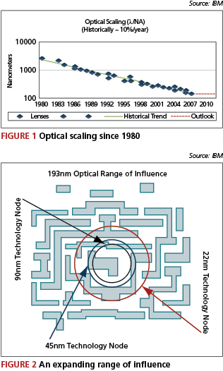
Operationally this has been accomplished by the periodic purchase of a new exposure tool and the optimized selection of wafer processing set points and mask types. As shown in Figure 1, optical scaling historically enabled a 10% annual reduction in feature size and an 81% annual increase in density through 2007. However, due to economic and technical issues, traditional scaling will not resume until next-generation lithographic (NGL) techniques such as extreme ultraviolet (EUV), nano-imprint and multi-column electron beam become available.
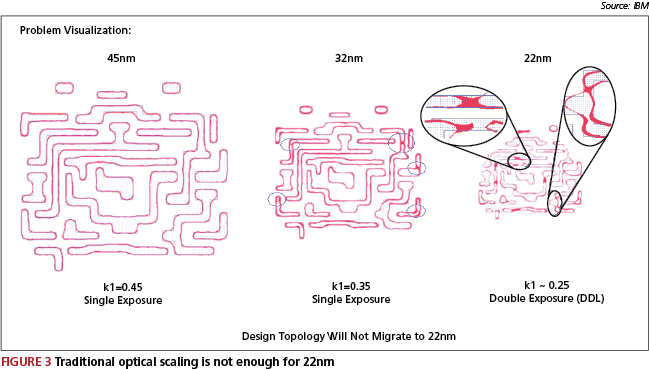
Although we have been able to realize a 10% annual improvement in optical scaling, this did not by itself support the two-year technology development cycle introduced in the late 1990s. As such, there has been a growing gap between desired optical scaling and realized optical scaling. One impact of this gap has been a decrease in the optical isolation of individual design constructs. The consequence, as shown in Figure 2, has been that individual constructs need to be viewed in the context of an expanding neighborhood.
The industry has managed this gap by introducing 193nm lithography, off-axis illumination, immersion lithography and double patterning. However, as shown in Figure 2, attempts to extend traditional optical scaling to the 22nm/20nm process node for a traditional 2D circuit pattern produce unacceptable results.
The current industry direction to address the highlighted problem at 22nm is the use of double (or triple) patterning with highly restrictive design rules (e.g., single orientation, near singular pitches, forbidden constructs) and design for manufacturing (DFM) tools that place responsibility for managing technological complexity on the shoulders of the designer. All of these approaches are driven by the increasing variance between designed 2D wafer patterns and resultant wafer patterns. Such a path drives a costly and complex departure from traditional IC design migration paths and increases the cost of wafer production for the fabricator.
Design implications
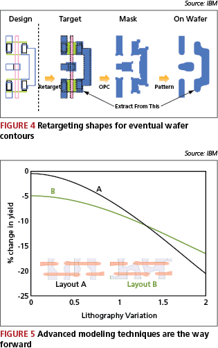
The first important point to observe is that because l/NA has not been scaling consistently with incoming geometries, the radius of influence for lithographic concerns has been growing in terms of design features. This problem is illustrated in Figure 3. In the past, this radius might cover at most a nearby edge pair, so width/space rules were generally a sufficient response. As this radius has grown, the complexity of rules has grown as well, resulting in width-dependent space rules and other multiple edge constraints.

At the same time, the typical curvature introduced on the wafer has become comparable to feature size, so that it is no longer reasonable to assume that wafer contours will essentially resemble the original drawn shapes, except for some minor corner rounding. It is necessary therefore to consider patterns of larger radius, and correspondingly less detail.
A second concern is that the various lithographic solutions available are not simply ordered. Any given approach to sub-wavelength lithography favors some classes of layouts at the expense of others. It is critical to work with design evaluation processes that will lead to the selection of that technique that best fits your design. For example, a strong dipole is good at printing parallel lines in one direction at certain pitches. But that comes at the cost of wires in the other direction. Pushing the minimum pitch may also introduce dead zones of forbidden pitch. Going to multiple exposures introduces further trade-offs. Does one use the second exposure to print alternating lines at a tighter pitch at the cost of the other direction, or print both directions with a more relaxed pitch, or enhance the printability of difficult 2D situations?

A helpful concept here is the idea of retargeting (Figure 4). This involves the adjustment of drawn shapes to serve as targets for eventual wafer contours. Of necessity, this is already happening to print certain features, such as isolated lines. But it can also be exploited to simplify the design representation. Given the flexibility to adjust shapes so that they satisfy manufacturability needs, a design can be represented on a coarser grid, capturing the topological intent without undue attention to fine details of edge movement, and without the need for identifying or following an inordinate number of rules when such small movements are allowed.
Density needs can be assisted by the identification of prevalidated constructs, consisting of topologies not generally allowable, but manufacturable in certain well-defined contexts with certain specified retargeting (cf, SRAM cells but in the context of logic cells). A close design-technology interaction is required to make sure such constructs are properly validated along with ordinary content, and defined for maximum utility to design. Updates to this methodology are likely, but much of the infrastructure is already present in the form of parameterized cells.
It is helpful when thinking about these concepts for design and design automation to consider the design community as falling into two camps. One is made up of those who use technology to produce full chip designs. The other comprises those who work with technology to define its character. The first group is increasingly focused on productivity, away from detailed layout and toward automation, micro-architecture and the balance between power and performance. The second is aware of technology limitations and uses tools like lithographic simulation to evaluate the trade-offs between manufacturability and design issues like density, rule complexity and design methodology.
For the first community of chip designers, the overriding technological direction is fairly synergistic and transparent. More design will be prevalidated in cell libraries and other building blocks. Wiring level rules will be evaluated for designability (i.e., friendliness to router technology), making automation more likely. And an early focus on high value patterns (with detailed implementation left to technology) should reduce the risk of significant layout change late in design. Moving toward more regular design rules should also contribute to this simplification, removing the need for this community to worry about detailed edge movements.
There are some areas that could affect the first community, depending on how the design rules evolve. One clear example is the anisotropy in wiring levels. Lithographic solutions often strongly favor one direction, so wire pitch and width values will differ depending on the preferred direction. The value of patterns in expressing design constructs and layout issues suggests opportunities to impact productivity by exploiting such patterns in construction (routing, cell assembly) or analysis (extraction, rule checking) tasks. For example, technology could directly deliver router building blocks rather than delivering edge rules that the router configuration must experiment with to produce useful router rules. Cell assembly could use predefined blocks to achieve better density but still maintain a coarse topological grid. Extraction could use look-up for predefined content to improve accuracy and runtime, and access a retargeting process to improve accuracy.
The second community of designers contributing to technology definition is more obviously affected by the emerging discontinuity. More prevalidated content will be developed (similar, again, to SRAM cells today), with simulation validation and advanced lithographic techniques as illustrated in Figure 5. The modeling of all aspects of the manufacturing flow (in addition to lithography) will need to improve to allow trade-offs to be made intelligently with simulation.
Design and technology will need to develop efficient means of communicating: technology simulation and uncertainty to design, and design evaluations and proposed content to be added to technology offerings. Some aspects of the handoff between design and technology may evolve as a result (e.g., delivering patterns for predefined content rather than rules, or delivering router configurations directly). The involvement of design will occur earlier in a technology node, to help make the difficult decisions among the unavoidable trade-offs. New mechanisms for expressing design intent (beyond just drawn shapes) can enable technology to further optimize the contours for added value (yield, density, power
-performance).
Summary
Severely sub-wavelength lithography presents some unavoidable conflicts with traditional scaling assumptions. However, disciplined design-technology co-optimization provides opportunities to define effective value by carefully considering the necessary trade-offs early in the technology cycle. Design communities will be affected differently based on their interaction with technology.
Chip designers will see fairly evolutionary changes, with more regular design rules, perhaps supplemented with patterns of predefined content in constrained situations. Designers working with technology will have an increased ability to influence its direction by understanding trade-offs and working to optimize design value. IBM is engaged in all aspects of this in delivering its computational scaling solution, and is working with its partners to deliver valuable manufacturable technologies in this deep sub-wavelength realm.
References
[1] “IBM Develops Computational Scaling Solution for Next Generation ‘22nm’ Semiconductors”, press release issued 17 September 2008 (access online at http://www-03.ibm.com/press/us/en/pressrelease/25147.wss).
IBM Microelectronics Division
East Fishkill facility
Route 52
Hopewell Junction
NY 12533
USA
W: www.ibm.com


