The challenge of analog, mixed-signal and custom physical implementation at 28nm
The 28nm process node has once more raised the design bar in terms of the DFM checks needed to realize a design. This is particularly true for analog and mixed-signal engineering, where rules that could once be maintained manually now need to be addressed in a more integrated, automated, and timely way. The article explores the challenges 28nm presents and describes the kind of design infrastructure needed to overcome them.
Size. Complexity. Size. Complexity. As we go from one technology node to the next, we seek to fit the same functionality in a smaller area, or, more likely, more functionality in the same area. But so what? Well, the width of a human hair is about 100,000nm. Now go back to four words in the title of this article: “physical implementation at 28nm.” Doesn’t it just boggle your mind?
Why is 28nm any different from 90, 60, or 45nm? Well, in some respects, it isn’t. We first started encountering a fair number of the issues discussed here at 130nm. However, some that started out as second- and third-order effects have become serious concerns. Additionally, entirely new effects have emerged at 28nm. As a result, existing design and verification techniques are starting to fall short. The sky isn’t falling, but this node still presents a much greater challenge than its predecessors.
The state of custom design
For some years now, mobile consumer products have been driving design starts, especially for leading-edge technologies. Anyone with a cell phone is aware of how fast and furious change has been—functionality and performance seem to expand exponentially with each new product generation.
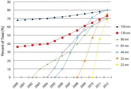
Many people still associate electronics primarily with digital technology, but the analog and mixed signal (AMS) content in these products has also grown with every new node. In fact, nearly 70% of today’s designs can be considered mixed signal (Figure 1). Radios, sensors, I/O, controllers, power management—all require or provide interfaces to or from variable power and signal sources.
Figure 1
Mixed-signal design starts by technology
Source: Mentor Graphics
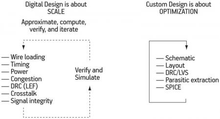
Digital design is all about scale. To realize chips with billions of transistors, engineers use approximate models for wire loading, timing, power, and more. In the digital world, design rules are approximated by the rules that can be coded into the LEF technology. Designers can then simulate and correct their work as necessary during the signoff design rule check (DRC) process. By contrast, custom design is all about optimization. Engineers must perform design and layout with the most accurate tools available, because that last 1%, or even 0.5%, of improvement is often critical to achieving the desired performance specifications (Figure 2).
Figure 2
Differences between digital and analog design flows
Source: Mentor Graphics
This difference in emphasis also affects the roles people play in the design process. In digital design, the physical design (place and route) is largely automated, and most human resources are directed toward set-up of the tools, evaluation of the results, debugging, and fixing. In custom design, engineers are an integral part of the design of the layout at every step of the design and verification process. Therefore, early feedback on manufacturing issues has to be provided in a way that is understandable to those human engineers.
What’s different at 28nm?
Everyone knows that with each new process technology, the number of transistors per unit area doubles. However, the typical area of a chip has remained more or less the same. Designers use the extra real estate to add more functions—Bluetooth one year, Wi-Fi the next, streaming video after that, and so on. As a result, the layout data for a chip design also doubles with each new node.
In addition to the direct doubling of layout density, each new technology is more difficult to manufacture than the one before. Ideally, the foundries solve the technology issues and provide a stable, competitive process that can handle any design—and they do overcome an impressive number of difficult technical issues. However, there will typically be a set of ‘marginalities’ that the foundries cannot fix for every possible implementation, at least not cost-effectively. These marginalities become new design rules and layout-dependent transistor effects. Thus, sign-off DRC decks grow and grow with every node. Like taxes, once created, design rules never go away.
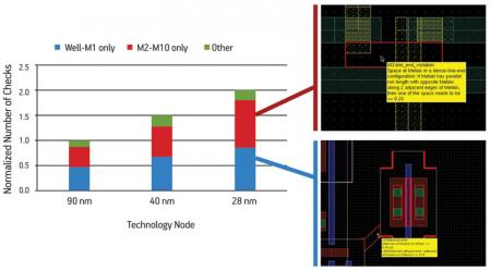
The total number of design rules has doubled between 90 and 28nm, and rule complexity is outpacing that for both LEF rules and the built-in DRC checkers provided with custom design tools. A growth in metal rules is partially due to an increasing number of metal layers. But the front end—where AMS/custom designers spend most of their time—has seen growth at the same rate without any new layers being involved (Figure 3, p. 42).
Figure 3
Growth in signoff DRC rules and complexity
Source: Mentor Graphics
Not only are there more rules, but these rules are becoming ever more complex. For example, where there used to be a single type of via enclosure, there can now be five or more, depending on the local environment. At the front end, transistor rules now have to deal with complex local interactions involving multiple layers, some of which are not even drawn, making it difficult for the layout engineer to understand why a transistor is ‘bad’.
The DRC checkers built into AMS/custom design tools are designed to assist with simple design rule specifications such as minimum width or space. Historically, custom designers simply memorized the rules not included in their tools, largely because they could—at 90nm, it was a short list. At 28nm, it is much longer than designers can cope with, if they can even understand the rules, given the complexity they now encapsulate.
Today, rules address such challenging requirements as multi-dimensional width/spacing interactions; ‘keep-away’ zones that aim to minimize the lithographic impact on transistor performance or reliability; and pitch checks that make printing easier and more consistent. Context can be as important as the actual configuration. While built-in DRC checkers, constraints, and LEF rules are continuously being expanded to increase coverage, it is a full-time job to keep up with the leading edge of technology in its entirety.
AMS/custom designers have historically implemented layouts using a combination of manual and automated techniques, and then run large sections of their layouts through full-chip verification in batch mode. They have fixed resulting DRC errors and applied DFM optimizations, then moved on to the next section of the layout and repeated the process.
This worked fine when designers could understand the issues, correct them, and get to closure within a few iterations. However, as the DRC/DFM rules have become increasingly complex, the number of DRC violations and DFM recommendations has also increased, requiring more time to be spent debugging and correcting the design. Debugging itself is getting trickier—in some cases, the fixes applied by designers introduce new DRC errors that are not identified until a subsequent batch verification run. With the number of iterations rising, tapeout schedules have started to slip.
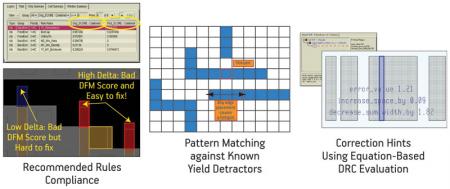
Full-featured DRC/DFM engines employ sophisticated techniques (Figure 4) to help engineers evaluate and optimize designs. With access to a fully featured DRC engine, they can take advantage of such advanced capabilities as equation-based DRC to obtain precise information about the error condition and any necessary corrections, and also pattern matching that identifies known problematic configurations. In addition, automated evaluation against a qualified deck of recommended rules enables designers to quickly prioritize changes that will improve areas particularly susceptible to manufacturing defects.
Figure 4
Full-featured DRC/DFM engines offer a variety of techniques and information to assist designers during debugging and design optimization.
Source: Mentor Graphics
Process simulation, in the form of model-based tools, has long been employed by foundries. Simulating processes such as lithography or planarity helps predict design failures that will result from specific process conditions. This technique proved so useful at 40nm that foundries now recommend (and in some cases require) the use of such models alongside DRC within the design flow. Houses that do not implement model-based DFM can encounter performance issues or variations in yield caused by design conditions that could have been corrected during layout.
At 28nm, fill is no longer a simple check-box task. Smarter solutions are needed to manage issues arising from tighter spacing. These include poly and metal density variation, multi-dimensional planarity interactions, and the impact of fill on timing. Advanced fill techniques can both prevent defects by maintaining better planarity and improve parametric yield by introducing less parasitic capacitance.
There has also been considerable discussion about whether timing-aware fill is needed at 28nm, that is, is it necessary to incorporate final GDSII fill data into the extraction and timing analysis flow to ensure that the final manufactured layout meets performance goals? On the other hand, even if the designer goes to the trouble to insert, optimize, and characterize fill during the design phase, can the foundry afford to let customers have final control over a step that is so critical to the manufacturing yield? Will the foundry use their own sophisticated solutions to replace customer-provided fill in some designs?
Double patterning has been identified as an enabling technology for 20nm and below, meaning designers must be able to analyze their designs for both patternability (whether or not a single layout structure can safely be decomposed into two masks) and composability (whether or not combinations of configurations in a complete layout remain decomposable). This new requirement makes layout even more challenging.
The complexity of all of these technologies, and the tight correlation they must maintain with foundry data and processes, makes it unlikely that AMS/custom design tool vendors will implement the full range of tools and technologies available in full-featured DRC/DFM engines. Even if the vendors wanted to provide signoff verification in their internal DRC checking, it would not make much sense. AMS/custom design tools are intended to make layout engineers more productive, not perform signoff verification. Providing signoff verification requires extensive and continuous interactions with foundries to ensure that the latest process requirements and interactions have been identified, categorized, and translated into a complete set of design rules and checks that ensure design compliance means manufacturability.
The end result is that we now have a significant gap in the custom design process that is impacting the quality and capability of AMS designs from 28nm and below. So how are custom designers coping? In general, their responses fall into three categories:
- Less optimization—designers are stopping as soon as they get to a DRC-clean design. However, they know they are leaving quality and performance enhancements on the table, which means they are also surrendering some competitiveness. They know this will hurt profit down the road; what they don’t know is when or how.
- Longer production schedules—some design teams opt to let milestones slip so that they can undertake additional optimizations. However, this strategy only works for a limited period of time for both individual designers and design companies.
- Staff augmentation—design houses are adding layout engineers. While this approach enables more work to be done without a change in methodology, it is a costly solution that does not scale well, even if companies pursue least-cost engineering resources.
None of these approaches solves the underlying problem—the inability of designers to access the full range of DRC and DFM methodologies concurrently with design layout implementation. Designers have their own bandwidth restraints too—they can deal with a lot of simple rules or a few complex ones, but not a lot of complex rules all at the same time.
What can we do?
As discussed, DRC and production schedules are not the only challenges here. Foundries are expanding tapeout requirements to include such processes as pattern matching, process simulations, and recommended rule compliance. There are new manufacturing requirements such as double patterning being added to the design team’s list of responsibilities. As a result, converging on a tapeout design while maintaining production schedules is getting harder and harder to reconcile.
As we reach 28nm, it would seem that designers are better off using the same
signoff tools used by the foundries to ensure concurrence between design layout checks and silicon results. However, without real-time access to the tools and techniques discussed above, custom designers will always be fighting a losing battle against both design quality and time-to-market.
Using industry interfaces such as the OpenAccess Run Time Model, it is now possible to embed a signoff-quality DRC/DFM engine in custom design tools to run DRC and DFM analysis in real time. This provides immediate feedback on each shape as it is incorporated into the layout. With sufficient speed, such an environment can even provide visual cues that show the designers where a shape can be placed, or how dimensions must be optimized, during drawing.
By making signoff DRC part of layout creation, designers can work in confidence, knowing that they are checking configurations against foundry-qualified signoff rule decks. They can automatically map PDK layers to GDSII layers. Without the need to run multiple batch DRC/DFM verifications, and with more error information provided in the design environment, designers can have more time to implement design optimizations, while still meeting time-to-market schedules.
Mentor Graphics
Corporate Office
8005 SW Boeckman Rd
Wilsonville
OR 97070
USA
T: +1 800 547 3000
W: www.mentor.com


