Practical mixed-signal defect and fault injection automation and simulation
This defect and fault injection primer looks at how to standardize definitions, decide injection volume, measure activity, manage simulation, optimize test time and more.
Many IC designers want to verify the robustness of designs and tests by simulating them with potential defects or faults. The step can validate whether a design will keep operating as expected, or at least safely. This is key for automotive-grade designs. Simply put, a faulty condition cannot be allowed to put lives at risk; so designers can use fault injection to systematically verify how tolerant their designs are to potential issues.
The general idea of simulating designs with injected errors is not new, but doing so reliably and accurately via software automation remains tricky, especially for mixed-signal designs. Questions that arise are:
- What types of defects or faults should be simulated and how many?
- In what areas of the design should they be inserted?
- Are they effectively detected by the applied tests?
- How much testing is sufficient?
Digital logic designs have relatively well-known fault models; automated test pattern generation (ATPG) software tools have been targeting them for more than three decades. Analog and mixed-signal (AMS) circuits, however, have not benefited from such automation, at least to nowhere near the levels seen for digital designs. For mixed-signal ICs, test time for the analog portion can dominate total test time. For example, Figure 1 shows the test time distribution for a typical smartphone IC.
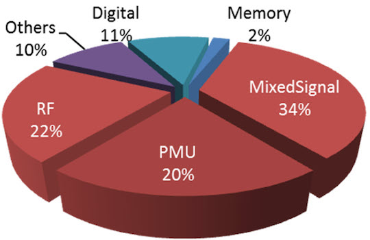
Figure 1. Analog test time dominates (Infineon Technologies)
Up until the last few years, defect and fault injection automation tools had to overcome several hurdles. Accurately simulating realistic analog faults is a computationally-intensive task typically done on a transistor-level netlist. Methods to get quicker results have historically included reducing the simulator’s precision, running simpler tests, using simpler defect models, or even just testing for a limited number of faults as time allowed before moving on.
Standardizing on defect/fault definitions
To be effective, an automated fault injection methodology must be based on industry-accepted defect models and also be flexible enough to support user-defined models. Such models allow manufacturers to enhance their verification processes by adding internally developed failure mechanisms typically derived from physical failure analysis (PFA) results.
Determining what the industry considers valid defect/fault models can be challenging. Fortunately, a recent IEEE proposed standard (P2427) formally defines a defect coverage accounting method based on simulation models for IC defects. The proposed standard is being developed by engineers from more than 20 major companies and is expected to be valuable to the entire design and test community. It enumerates the universe of potential defects, and how they should be reported in coverage results. Although P2427 primarily addresses analog defects, it also applies to digital circuitry (though simpler fault models are typically used for purely digital designs).
Having such a standard will very significant since it will pave the road to defect-oriented analog ATPG. It will provide a more deterministic way of estimating defective parts per million (DPPM) for ICs containing analog circuits. It will also establish a common methodology for reporting the coverage achieved by new tests and DFT to allow more objective comparisons.
Determining how many defects to inject
With defect and fault models now agreed upon, the next step is normally to list the potential defects for a given design and then insert and simulate them one-by-one. The procedure can be applied exhaustively (i.e., by iterating through all potential defect locations), although doing so might require years of simulation before conclusions can be drawn.
In practice, it is sufficient to initially inject a small number of randomly selected defects – as few as 20. These simulations thus provide quick results about undetected defects with enough information to allow for quick analysis and improvement.
This in turn allows designers to spot test issues or missing test conditions. Existing tests can then be improved (and/or new ones added) to target the missed faults and others like them. As fewer and fewer defects remain undetected, coverage increases. When all of the selected defects have been detected, a larger number is selected for a more precise estimate of coverage.
How many such faults need to be injected? It is tempting to say ‘as many as possible’, but in practice it depends on the reported test coverage results and the confidence levels needed with those numbers.
Classical random sampling theory provides answers. Assume, say, that 95% coverage is reported after randomly injecting 250 defects, the 95% confidence interval would be ±4%. When injecting 1000 defects, this confidence interval would reduce to ±2%.
In other words, if the resulting defect coverage value is found to be 95% after injecting and simulating 1000 randomly-selected defects, the actual defect coverage (if exhaustively simulated for all potential defects) will land somewhere between 93% and 97%, for 19 circuits out of 20. Simulating more defects simply improves the confidence interval.
Measuring analog activity
Alongside the previously described strategies, there is another clever way to evaluate the effectiveness of an analog test without having to simulate even one defect. It is done by simulating a given test and analyzing the analog circuit elements that it actually exercises – thus effectively measuring the defect-free activity coverage of that test.
This innovative concept for analog circuits is akin to what digital logic designers call ‘toggle coverage’, but it considers circuit elements instead of logic gate outputs. If defect-free simulations reveal that a given test only exercises a portion of the design, then high defect coverage can only be expected in that portion. After all, if circuit elements are not activated by the test stimulus, any fault they might contain cannot be detected.
This new approach implies that without injecting any defect or fault, there is now a way to estimate the quality of analog tests. New tests can then be added (or better ones used) to increase activity coverage, if it is too low. After the combined activity coverage of those tests reaches a high enough value (which does not have to be 100%), defect and fault injection can proceed as usual.
Selecting which defects to simulate
Although less-capable EDA tools might consider that all defects and faults have the same occurrence probability, industry data shows this is not the case. For example, the longer two adjacent wires run next to each other in a layout, the more likely that a bridge occurs between them, and the higher the parasitic coupling capacitance. The possibility of a bridge occurring between those two traces will be approximately proportional to that capacitance.
A relative likelihood (RL) value can therefore be computed for every potential defect in a given design. This RL value is calculated using default design-specific metrics that can be overridden if needed (based, for example, on newer available data or rulesets). Defects having a high RL value are more likely to occur. Given limited resources, they should ideally be addressed by tests first, since covering them provides the biggest ‘bang for your buck’.
Using RL-weighted metrics provides an additional benefit: The overall coverage results reported from simulations can be more precise for a given number of selected defects. For industry-reported defect likelihoods, mathematical analysis has shown that using RL-weighted defect sampling leads to the same confidence intervals as simple random sampling while requiring only one-fourth the number of defects to be simulated.
This means, that when reporting a 95% coverage result simulating 250 RL-weighted defect samples is statistically just as good as simulating 1,000 simple randomly-selected defects.
Understanding defect tolerance and functional safety
A key application for injecting faults is to validate the defect tolerance of a design and whether it remains functionally safe as it operates.
Adding redundant memory elements in a digital IC is a typical example of defect tolerance: If a memory is found to have defective locations during its manufacturing tests, a repair code can be applied so it uses its redundant elements instead (assuming they are not defective as well).
If a design cannot be 100% defect-tolerant then it cannot be safe. But for automotive designs, the ISO 26262 standard requires ICs be safe, which means a ‘safety monitor’ is needed to periodically check whether a fault has occurred in the function. In such a case (and depending on the fault’s seriousness) a safe state must be entered to minimize risks to the vehicle’s occupants and anyone nearby.
Defect injection can be used to validate that any faulty analog circuit keeps operating within safe limits or, if an output falls outside the predetermined safe range because of a defect, that the safety monitor detects it and acts accordingly.
To assess this functional safety, ISO 26262 defines various defect tolerance metrics (e.g., percentage of safe or latent defects, safety monitor defect coverage, diagnostic coverage, non-latent defects). An automated defect/fault injection solution should therefore directly report all key ISO 26262 metrics, rather than requiring designers to manually assess them.
Optimizing test time
Digital logic test pattern sets are usually scrutinized to ensure that the test time they require is well spent. However, industry data shows that analog and mixed-signal test time represents the vast majority of all IC manufacturing tests. Why is analog test time optimization versus defect coverage not a highly debated topic?
A potential explanation is that until very recently objectively determining the effectiveness of analog tests was nearly impossible given the lack of formal defect/fault definitions and related coverage measurement methods.
Given that standard defect and fault models were proposed and that activity and fault coverages can now be precisely computed, determining whether a given analog test truly provides additional coverage becomes practical; you do not have to test millions of devices first. If it only detects the same defects and faults that were identified by preceding analog tests, why run it? Such a test wastes valuable time.
Using Tessent DefectSim
In successful use by designers for several years, Tessent DefectSim (Figure 2) provides transistor-level fault simulation for analog, AMS, and non-scan digital circuits. It is used when test quality must be measured or improved, or when quality must be maintained while test cost is reduced. DefectSim automation replaces manual assessment of test coverage and safety-related metrics in AMS circuits, which is needed to meet quality standards such as ISO 26262, and provides objective data to guide improvements in design-for-test (DFT) and fault tolerance.
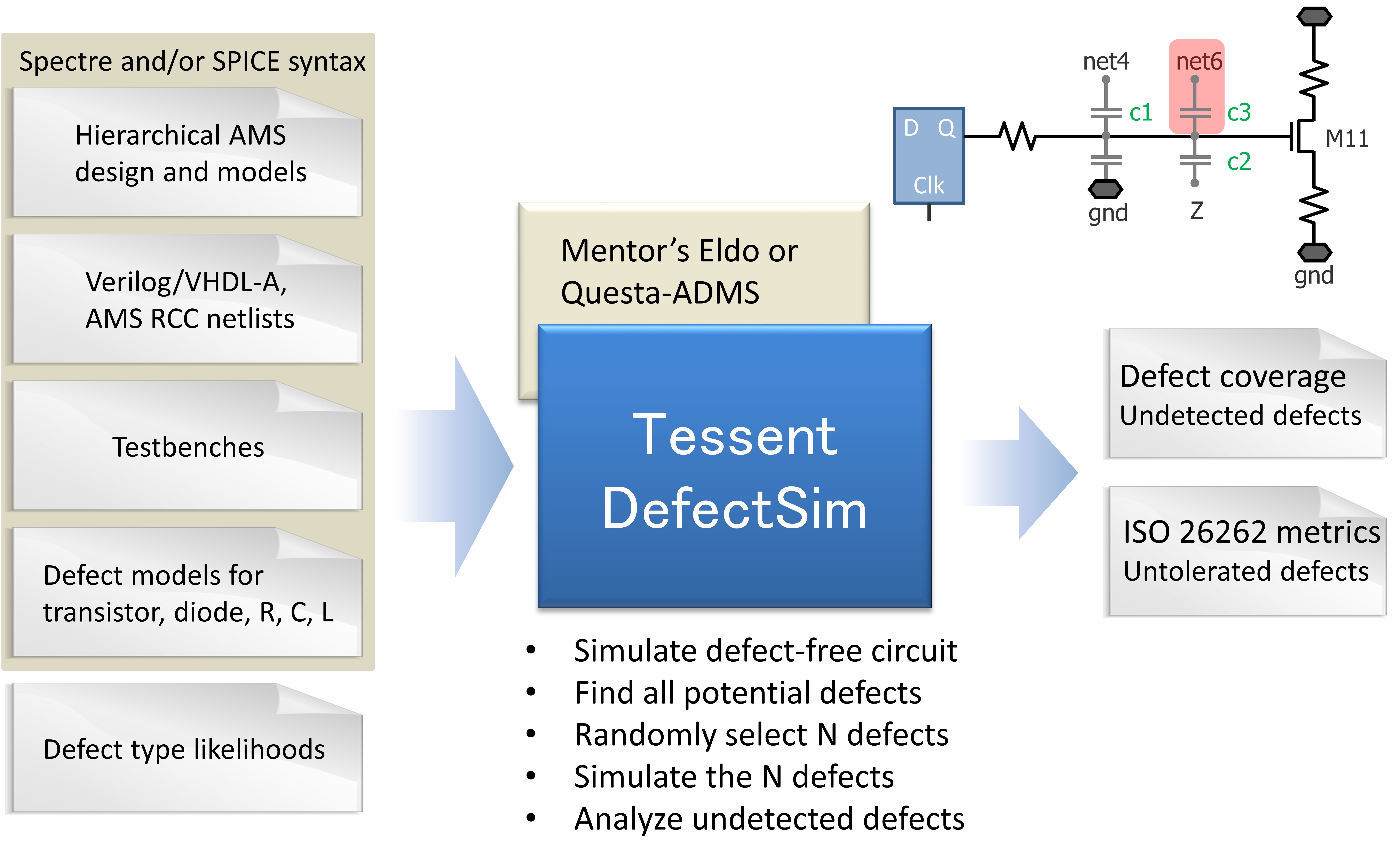
Figure 2. Tessent DefectSim flow (Mentor – click to enlarge)
The key features of Tessent DefectSim include:
- Measuring the likelihood-weighted coverage of defects and defect tolerance in AMS circuits.
- Injecting realistic shorts, opens, variations, IEEE P2427 defects, and user-defined defects and faults.
- Reducing simulation time by orders of magnitude compared to simulating a production test for each possible defect in a flat netlist.
- Simulating any combination of Spectre, SPICE, and HDL models, analog/digital circuitry, pre- and post-layout subcircuit netlists.
- Measuring all ISO 26262 metrics.
The takeaway
By combining RL-weighted sampling with other proven speedup techniques, DefectSim combined with a simulator can report accurate analog test coverage metrics more than a million times faster than performing an exhaustive simulation of all potential defects and faults in a flat layout-extracted transistor-level netlist. It does this without sacrificing test quality, accuracy, or a reliance on simpler (hence less realistic) fault models.
Designers can now rely on such automation to make sure their AMS designs are defect-tolerant and will keep operating within safe limits. The automation generates key ISO 26262 metrics, so engineers do not have to manually compute such critical data. In many cases, it is possible to assess these metrics while simultaneously measuring the defect/fault coverage of manufacturing tests.
This makes defect and fault injection in analog designs possible and practical. Using standardized defect/fault models from IEEE P2427, DefectSim can objectively and comprehensively report analog test coverage metrics. Test engineers now have a way to assess the quality of analog tests and can determine if manufacturing test time is optimally spent.
A new metric (activity coverage) estimates the maximum coverage that a given set of tests provides, without injecting any defects or faults in the circuit netlist. This alone can guide AMS designers in making improvements to their manufacturing tests, resulting in fewer analog test escapes and safer designs.
To learn more, check out this whitepaper: Analog Fault Simulation Challenges and Solutions.
About the author
Etienne Racine is a Technical Marketing Engineer at Mentor, a Siemens Business.