Solving the next parasitic extraction challenge
A greater proportion of the layout requires more precise extraction at the 32nm and 28nm process nodes, so rules-based extraction tools can no longer deliver the accuracy needed to confirm acceptable electrical performance. Given the nature of parasitic elements in analog and mixed-signal (AMS) system-on-chip designs, designers need a parasitic extraction tool that provides gate-level, transistor-level and mixed-level analysis, plus accuracy, capacity and scalable performance. A parasitic extraction tool that includes field-solver accuracy with production-level performance and turn-around time will enable designers to achieve design closure and gain confidence that their ICs will function when manufactured. Ideally, the result will be AMS SoC designs that meet operational specifications, use space more efficiently, and perform even better.
The Semiconductor Technology Roadmap [1] describes the problems that need to be tackled for future generations of silicon technology. The report illustrates the electrical and manufacturing characteristics for processes and the problems that can affect the success of adopting future nodes. Shrinking device sizes and finer line widths allow IC designers to pack more functionality onto a chip, but this has also generated a new set of design closure problems that must be dealt with. This is especially true for complex analog/mixed-signal system-on-chips (AMS SoCs) where sensitive analog circuits are particularly susceptible to noise and the effects of parasitic resistance and capacitance.
As IC designs move through each successive process node, smaller dimensions lead to increased interaction among transistors in ever closer proximity, as well as between transistors and interconnect layers. Parasitic circuit elements are increasingly affecting performance. Thus, they must be modeled much more accurately at 28 and 32nm than was the case at 130nm or even 65nm.
The inputs for simulation are derived through ‘extraction’, which converts the physical design after implementation back into representative electrical circuit elements. In other words, extraction measures the actual shapes and spacings in the lithography mask layers and predicts the resulting electrical characteristics of the manufactured chip.
This is a two-step process. The first part of the process is ‘device’ extraction. It identifies the circuit elements (e.g., transistors, diodes, spiral inductors, etc.) that the designer intended to form the circuit implementation. The second part identifies the electrical characteristics of the wiring (or routing) that connects these elements together. This step is called ‘parasitic’ extraction because the electrical characteristics of the wires (resistance, capacitance and inductance) are an unwanted byproduct of wiring but nonetheless impact circuit performance and need to be accounted for.
In addition to unavoidable parasitics, manufacturing variation also impacts the performance of devices and wires. All of these factors must be accurately characterized to determine silicon performance. It is the job of extraction and simulation tools to accurately convey this information and help designers determine whether they will hit or miss performance expectations.
Traditional extraction
Extraction of the R, C and L circuit values can be done at varying levels of detail. At nodes from 65-130nm, detailed extraction is usually performed only on the interconnect wires, because it can take too long and cost too much to compute the overall capacitance for all the devices and transistors in a design. Extraction at these nodes determines the resistance of the wires and the parasitic capacitance between the wires that affect circuit timing and the performance of the whole chip.
To facilitate fast extraction run-times, full-chip interconnect models are placed in a database using specialized layout extraction software. Rule-based extractors then use these models in conjunction with layout pattern recognition algorithms to compute capacitance values for the interconnect. This parasitic data is qualified against known ‘golden’ data obtained from either a 3D field solver or measurements on silicon [2] (Figure 1).
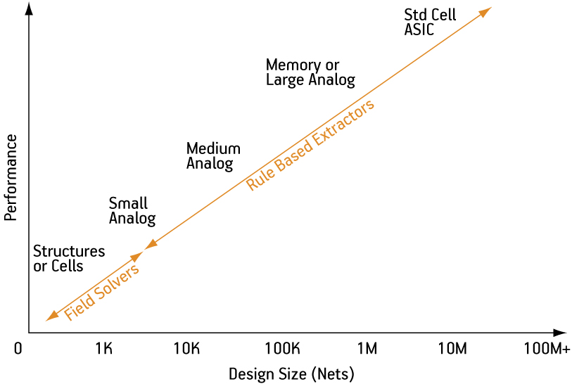
Figure 1
Rule-based extraction tools have high-performance, but compared to field solvers are not accurate enough for advanced nodes (32/28 nm and smaller)
Source: Mentor Graphics
Performance vs. accuracy trade-off
More accurate extraction and simulation allows designers to use smaller, more realistic design margins, resulting in more competitive IC performance specifications. Traditional rule-based extraction methods relied on heuristic models (approximations) that are inherently limited in accuracy—as much as 10% error for total capacitance values, and up to 15% or more for coupling capacitance (Figure 2). Because of these extraction errors, there is more uncertainty in the simulation results and larger design margins are required.
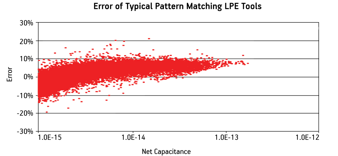
Figure 2
The margin of error in traditional rule-based extraction tools can be 10-20%
Source: Mentor Graphics
Extracting device-level parasitics is becoming more of an issue at the 32nm and 28nm nodes. The device models at advanced nodes have been changing, and more capacitive effects are modeled as parasitics. This means that in addition to extracting large capacitance values (e.g., on long CLK lines), extraction tools must also consider attofarad-level capacitances for individual effects around a transistor. New techniques need to be employed by extraction tools if they are going to address the advanced effects and reduce the error.
Solutions based on field-solver technology, instead of heuristics or rules, are inherently more accurate because they use Maxwell’s Equations to compute the electrical field at each point in a 3D space. Field solvers have been shown to deliver accuracy on the order of 2-3% error, but also have historically been orders of magnitude slower than rule-based approaches, making them impractical for production use.
At nodes below 28nm, design teams require accuracy close to that of 3D solvers, but must still be able to manage the run-time using hierarchical strategies and by partitioning the task over a large network. In particular, 3D extraction accuracy is needed for the clock tree and the devices in critical cells, such as a SRAM bit cell.
Although the big players in the EDA market for parasitic extraction solutions have been providing traditional rule-based production extraction tools for quite some time, they have been introducing 3D parasitic extraction tools based on field-solver technology to address the need for even greater accuracy. Some of these newer tools use statistical (Monte Carlo) techniques to improve extraction accuracy. These solutions, although nearly twice as accurate as the older tools, are not scaling with performance—that is, run-time increases exponentially with increased accuracy, which means that run-time performance degrades quickly as accuracy requirements increase. In addition, with statistical techniques, there can still be outliers in the results, and the results are not repeatable when moving from one run to the next on the same chip.
The future of extraction: accuracy plus performance
Accuracy is not the only important factor to consider when it comes to extraction. There is a need for high accuracy for both interconnects and near devices (transistors), as well as good performance that scales linearly with accuracy (Figure 3). Results should be repeatable to be assured of accuracy as well as reliability, and statistical outliers need to be eliminated because they can lead to catastrophic errors in the chip analysis.
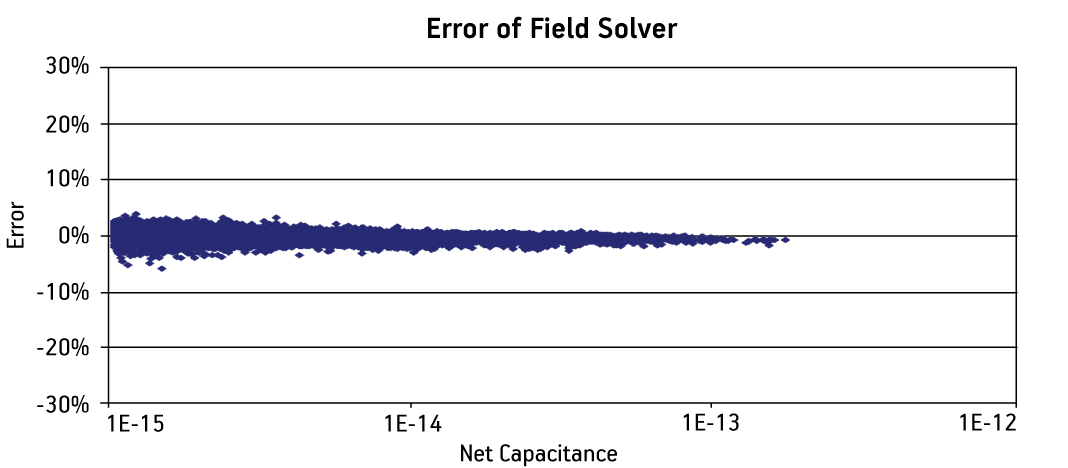
Figure 3
A field solver or 3D extraction tool for designs at 32/28nm should have a margin of error less than 5% and a reasonable cycle time
Source: Mentor Graphics
Run-times for parasitic extraction also need to be reasonable to ensure the designers are not operating on old layout data. Because a design with 500K devices may have multiple designers making changes, data must be refreshed frequently. The design team needs to be able to find and fix timing errors and failing nets confidently. And the sensitivity of parasitics to process variations has to be understood to reduce yield loss.
At smaller geometries, interactions that used to be ‘second order effects’ become much more important. Everything is closer together, so field effects have more influence on neighboring structures, and the effects extend over a wider context (i.e., greater number of adjacent transistors). At 32nm and beyond, transistor-level accuracy demands are increasing.
Transistor-level designers consider accuracy to be their first priority, but they also want full chip speed and capacity. On the other hand, gate-level designers consider speed and ease of use to be more important; however, they also want bounded +/-10% accuracy. Whatever the priorities, once the design’s transistor sizes drop below 28nm, it is critical that the design team can perform accurate, full-chip, distributed and coupled RC extraction for delay as well as signal noise, clock skew, IR drop and electromigration analysis—and do so in a reasonable amount of time.
Extraction tools that include all major effects such as in-die variation and inductance while generating consistent and repeatable results with reasonable run-times, will be more useful than those that focus on high accuracy alone.
Even with greater demands being placed on transistor-level extraction, an extraction tool must still work very closely with the layout-vs.-schematic (LVS) tool, because the process uses a combination of models that reside partly within the LVS tool and partly within the extraction tool. So whatever extraction and LVS tools are used, they must be designed so that they work well together.
References
- The International Technology Roadmap for Semiconductors, http://public.itrs.net/about.html.
- “A Practical Approach to Parasitic Extraction for Design of Multimillion-Transistor Integrated Circuits”, John MacDonald, Lakshminarasimh Varadadesikan, Wieze Xie, Eileen You, Proc. 37th Design Automation Conference (DAC ‘00), pp.69-74.
Mentor Graphics Corp.
Corporate Office
8005 SW Boeckman Rd
Wilsonville
OR 97070
USA
T: +1 800 547 3000
W: www.mentor.com