Silicon test moves up the food chain
Technological advances are often driven by the need to simplify and control a task. Silicon test is a good example. Its requirements are continuously increasing in complexity and this process drives the development and adoption of automated test strategies.
A thorough approach to manufacturing test is essential to the delivery of high-quality devices. A whole-chip test methodology must address logic, memory, clock generation and I/O access. You need to vary the test types and their application methods used, and also fully analyze early silicon and yield-limiting defects. These various and increasingly complex requirements make automation necessary.
This article discusses the move to automated tools to support the test methods, flexibility and defect analysis necessary in today’s mixed-signal system-on-chip production environment.
The silicon test process continues to become more complicated as both integration and fabrication technologies develop and new defect mechanisms emerge. Not only must it detect subtle flaws in random logic, but it also must extend to all other major areas on the silicon, including various types of memory, clocks and high-speed I/Os. It must also encompass multiple stages in a device’s development cycle such as first silicon debug, burn-in and field test. For complex devices such as mixed-signal system-on-chips (SoCs), having to manually develop test patterns or design and insertion logic to ensure the application of high-quality tests is a daunting, and often unrealizable, task. Effective automation is vital.
Automation to date
Whenever design tasks have become too complex or time-consuming, EDA tools have been developed in response. Obvious examples include the challenges posed by schematic capture, synthesis, and place and route. Silicon manufacturing test has already encountered many situations where complexity has made automated solutions an absolute necessity. Such instances include boundary scan, internal scan and memory built-in self-test (BIST).
Automated scan test became necessary when gate counts reached levels where it simply became too difficult to manually produce a high-quality pattern set that would detect most defects. The automated insertion of scan logic and corresponding automatic pattern test generation (ATPG) offered in commercial tools have turned scan test into standard practice. The process is now so well automated that very little knowledge of the design is needed to ensure the application of high-quality static tests.
Here are some of the areas where manufacturing test automation is today commonplace.
- Embedded test compression: This technology enables scan test pattern application up to 100 times faster than a traditional scan pattern set with correspondingly fewer tester cycles. It permits the use of many additional pattern types for small geometries and fewer pins in the test interface without changing the properties of the tester or increasing the test time. Because of automation, the design of embedded compression logic and test pattern generation are transparent.
- Pattern generation automation: This started to require more manual settings as design complexity increased. As various options and features were added to ATPG tools to handle various design styles, increasing expertise was needed to determine the appropriate settings. However, almost all the settings can now be reviewed and those that will give the best results implemented as the tool starts pattern generation.
- Logic BIST: This inserts embedded logic for a completely self-contained test. It provides a fully integrated test strategy that can be used at any test step or level of integration via a very simple interface. Processes such as logic insertion, problem logic fixes and test points for high-quality test are fully automated.
- Memory BIST: This inserts and manages self-contained tests for memory arrays. As with logic BIST, the logic insertion and testability fixes are fully automated.
- Memory defect analysis and repair: Memory built-in self-repair (BISR) automatically inserts logic for repair analysis to determine if a repair is possible and where it should occur.
New frontiers for automation
Today, the requirements and uses for test are expanding beyond random logic and memory test. The amount of clock generation and number of SerDes ports included in today’s devices adds significantly to the test burden. Consequently, BIST options for PLL jitter and SerDes ports have been added to the test automation portfolio.
Coverage analysis
If test insertion and pattern generation difficulties can mostly be addressed with automated tools, there remains a need to properly analyze the results and also any missing coverage.
The latter case is particularly challenging given huge levels of integration within a device. You can often be forced to set up multiple experiments to determine the causes of missing coverage or manually analyze a netlist to find logic that is interfering with coverage goals.
Source: Mentor Graphics
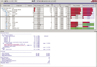
FIGURE 1 Automated fault analysis is embedded within test generation tools
In response, automated fault analysis features have been embedded within test generation tools. Analysis and experimentation is embedded in the ATPG process so that the summary report includes specific information about systematic as well as specific locations that are limiting test coverage (Figure 1).
Yield improvement
Silicon yield analysis has historically been based on basic test structure analysis and manual steps such as visual inspection. This approach can be very time-consuming, and it is tough to pick out systematic issues within what appear to be random data.
The population of defects caused by features in the silicon has grown with newer and smaller fabrication processes. Using existing scan and memory BIST results provides considerable insight into what is happening inside a failing device. Thus, automatic yield analysis tools based on failing scan pattern data or memory BIST data are becoming available. Many aspects of the early investigation, identification of outlier issues, and processing of large amounts of production data are automatically performed and reports produced in a very short time.
EDA software contains many test types and options for use when implementing test logic or pattern types. What is still needed is the flexibility to make adjustments after silicon has been produced.
Post-silicon test automation
Uncertainty about production defects and the need to get as much right as early as possible are more sensitive issues than ever due to incoming fabrication processes. There is also concern surrounding the impact of test procedures on power, switching, di/dt and power droop. Project managers want production tests that operate in as much the same way as possible as functional operating power and switching. Even with the automation we have available today, it can be hard to be confident that you have implemented all the tests a device really needs.
Source: Mentor Graphics
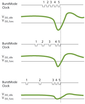
FIGURE 2 A programmable sequence of fast pulses during at-speed test lets you select the number of fast cycles before launch and capture without changing the pattern
The most important questions relate to what logic should be inserted so that the production test supports the desired pattern types. No one wants to be forced into considering a design re-spin because tests needed during production were not planned for sufficiently early in the design flow.
One solution is to build in such flexibility that experiments and test adjustments can be performed in software alone. The versatility to perform various tests is provided by automated test logic insertion. Memory BIST automation now includes features that allow new algorithms to be added to account for a defect type that was not originally foreseen.
Logic included in the test structures provides a custom-defined threshold that you can use to adjust the amount of scan shift activity as well as capture activity. In this way, you can tune the power impact of your tests on real silicon.
A recent feature available for test logic inserted for scan control is a programmable sequence of fast pulses for use during at-speed test. This logic keeps the pattern exactly the same but lets you define the number of fast cycles before the at-speed launch and capture. As a result, if you are concerned about power droop because only two fast pulses are together, you can specify that a number of the last few shifts will also have high-speed pulses. The result is a tunable test interface.
A form of automation is also available to simplify the types of experiments mentioned above and to provide a simple platform and interface through which to apply tests and adjustments. A link from a computer USB port directly to the device-under-test (DUT) is possible without the use of a tester. The computer interface is made through the boundary scan test access port (TAP) so that you can directly set up and apply adjustments to test parameters. You can make adjustments (e.g., which memory BIST algorithms to use, the number of high-speed shifts before at-speed launch and capture) directly to the device and immediately see the results. This interface can also be used for PLL or SerDes characterization, providing a simple platform to test and characterize PLL and SerDes in minutes instead of weeks.
Source: Mentor Graphics
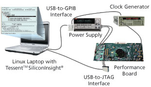
FIGURE 3 A simple bench-top platform and interface allows you to apply embedded tests and make adjustments through a direct link from USB to boundary scan on the chip
Test moves up the chain
Manufacturing test automation now encompasses much more than in the past. Complex requirements have driven more and more automation of the process to the extent that complete suites of tools are available to test all major areas of silicon. You can select the test methods and logic you want to use from a broad set of options. Test logic and generation have become the easy parts. But even the harder parts have been simplified by providing scope to make definable test adjustments on fabricated devices. You can experiment with memory algorithms, clocking, power and more, using a direct interface to the DUT. Production test patterns can be written based directly on these experiments.
With further automation, the expected test impact on a device’s production schedule will be greatly reduced while providing more options and significant capabilities to adjust for uncertainty in the test needs of fabricated devices.
Mentor Graphics
Corporate Office
8005 SW Boeckman Rd
Wilsonville
OR 97070
USA
T: +1 800 547 3000