Reducing test costs through multisite and concurrent testing
How to save test time and test costs by doing more tests in parallel, increasing compression, pooling tester memory, managing branching – and more
As the gate count of SoCs grows and the processes upon which they are built become more complex, the combination of more logic and increasingly subtle manufacturing defects means that more test data is needed to achieve higher defect coverage and lower defective parts per million (DPPM). More test data usually means more test time and cost.
Designers are using parallelism to fight back, cutting test time and so saving money. One way to do this is multisite test, which tests many die at once. Another is concurrent test, which tests multiple IP blocks on one die at the same time.
When testing digital logic, both approaches can take advantage of higher test time/data compression, faster scan shifting, and simultaneous test execution. Applying these techniques demands sophisticated test technology and infrastructure in the DFT software, the DFT IP on chip, and in the tester.
Multisite testing
As chips get bigger and quality requirements increase, test pattern sets are growing and so is the time it takes to run them, especially if the number of test pins is limited. One way to counter this trend is to use multisite test, which saves test time and therefore cost, by screening multiple chips at once.
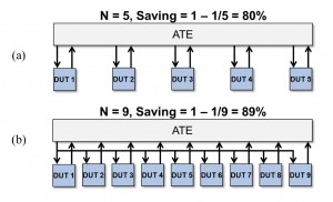
The number of die (or packaged parts) that can be tested at once (the ‘multisite count’) depends on the number of ATE channels and the number of test pins per die. The time saved, compared with a single-site approach, increases with the multisite count, N, according to the equation 1 – 1/N. For example, if the number of die tested at once is five, and there are enough ATE channels to accommodate the additional chip I/Os, the time saving is 80% (see Figure 1a).
Once all the ATE channels on the tester have been used, the next way to increase test parallelism is to use “stimuli broadcast”, in which the inputs to all the parts are driven by the same ATE channels, freeing up more resources to test additional chips. Now the multisite count can rise (to 9 for this example), making the time savings 89% (see Figure 1b).
Figure 1 Testing more sites at once saves test time. Scenarios (a) and (b) use the same number of ATE channels, but stimuli broadcast in (b) achieves greater parallelism. (Source: Synopsys)
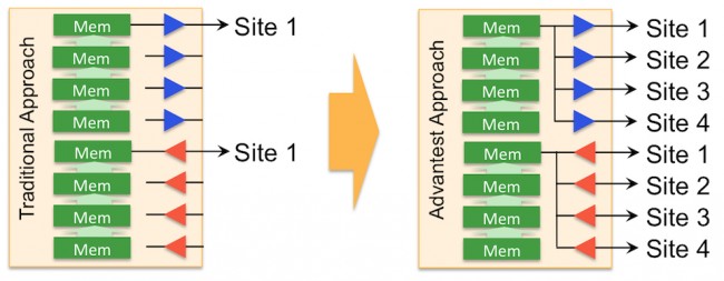
Some ATEs use memory-pooling techniques (see Figure 2) to enable deep pattern stimuli to be broadcast to multiple sites in parallel, leveraging electronics in each output pin to keep track of errors. This technique, which shares the same data stream on the inputs and tracks divergences from the expected results on the outputs, can give the tester the appearance of very deep per-pin pattern depths simultaneously on multiple sites (up to 32Gbyte per pin). Another advantage of this approach is it speeds the pattern downloads. When available, it’s a very efficient way to use ATE resources.
Figure 2 Memory pooling by the ATE can increase apparent pattern depth memory for each pin (Source: Advantest)
Real time savings and throughput
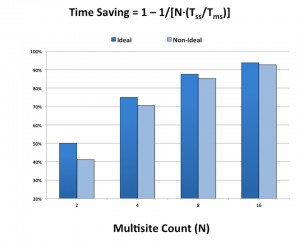
The examples of test time savings in the previous section are theoretical: the real time savings from applying these approaches are calculated in a more complex way. The average time to test each die using multisite test, Tms, is almost always greater than that for single-site test, Tss, so the time savings are actually less than implied by the equation above, as illustrated in Figure 3.
Figure 3 How theoretical multisite test time savings (dark blue) diverge from practical results (light blue) (Source: Synopsys)
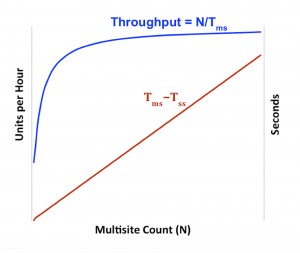
In addition, any effect that increases the multisite test time can also affect throughput, defined as the multisite count divided by the multisite test time, and measured in terms of units tested per hour. If the multisite test time per die continues to increase significantly with site count, the throughput can reach a point of diminishing returns, as shown in Figure 4.
Figure 4 The advantages of adding more parallel test sites can diminish as site counts rise (Source: Synopsys)
Multisite test time can increase for various reasons, including:
- problems with the probe card touching down on die at the edge of a wafer, which means that they have to be tested separately and/or repeatedly
- too few RF and/or mixed-signal test resources on the tester to support full multisite testing, because they tend to be more expensive than digital channels, limiting the amount of such testing that can be done in parallel
- the time it takes to position the probe interface to contact the bonding pads of the device under test
- branching in the test program flow, which can make one site’s execution time longer than another’s
Pin-limited compression: DFTMAX Ultra
Multisite testing demands better scan compression technology to drive the same amount of test vectors through the more limited number of test pins available per die in a multisite setting. We now describe the compression technology in Synopsys’ DFTMAX Ultra, and how you can use it to enable both multisite testing and concurrent testing.
Synopsys’ DFTMAX Ultra has been designed to achieve higher compression using fewer pins, so users can apply larger pattern sets, based on advanced fault models, to find subtle defects and reduce DPPM. The architecture is optimized to help TetraMAX ATPG manage unknown logic values. Built-in X-tolerance improves test coverage, increases compression efficiency, and enables accurate fault diagnostics. DFTMAX Ultra uses a streaming, bidirectional codec to simultaneously stream, decompress, and compress the test data, which eliminates the pipeline stalls between scan shifts that can happen using a SERDES-style implementation. Simpler scan-shift clocking enables high-speed shifting of scan chains on the tester to further cut test time and cost.
DFTMAX Ultra can use just one scan channel, plus a scan enable and clock, which saves pin resources and so enables more die to be tested at once, or more IP blocks to be tested per die. The tool is tightly linked with TetraMAX ATPG to generate patterns that limit both shift and capture power.
Implementing test compression
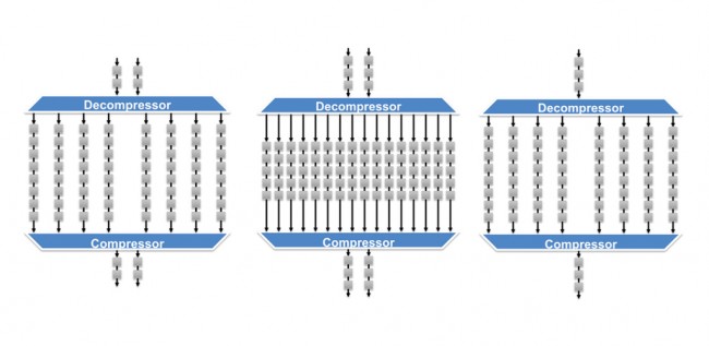
Reducing test costs through increased parallelism requires an intelligent trade-off of issues such as pin allocations, power, and tester resources. These trade-offs will then drive the overall test architecture, creating block-level constraints that will define the compression configuration for the DUT’s digital logic blocks. Figure 5 shows three possible architectures and related DFTMAX Ultra script.
Figure 5 Three combinations of chain count, scan in and scan out (Source: Synopsys)
The core-level DFTMAX Ultra insertion script that follows sets the number of inputs, short chain count, and the number of outputs (see highlighted line). In Figure 5, these ratios are 2:8:2, 2:16:2, and 1:8:1, respectively.
set_dft_configuration \
-streaming_compression enable
set_streaming_compression_configuration \
 -inputs 2 -chain_count 8 -outputs 2
create_test_protocol
dft_drc
preview_dft
insert_dft
write_test_protocol \
 -test_mode ScanCompression_mode \
 -out top_comp.spf
The last two approaches have the same scan-chain compression ratio (8x). DFTMAX Ultra offers virtually the same compression results when the scan chain ratio is the same, yet the scan channel count differs.
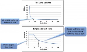
How much compression should be implemented? It depends on the amount of ATE memory allocated for digital test patterns. Take a hypothetical design that has digital logic and mixed-signal IP that needs to be tested (see Figure 6). In this example, the digital portion has millions of scan flops and thousands of ATPG patterns, which translates to about 17 times more data than can be allocated to digital testing, so the test patterns need to be compressed by at least this amount.
Figure 6 These charts show a hypothetical example of a design containing both digital logic and mixed-signal IP, both of which need to be tested (Source: Synopsys)
If 17x compression (i.e., a chain ratio of 17) were implemented in the design, then once the ATPG patterns were loaded into tester memory, it could still take nearly a minute to test the chip. To reduce this time, test engineers would need to increase the ATE clock rate to shift the scan chains faster, but this might not be practical due to power constraints.
An alternative approach would be to implement a higher chain compression ratio than 17x in the first place. However, if it is anticipated that the mixed-signal IP will be the test time bottleneck for the design—taking, for example, 30 seconds to test—then the chain ratio needs to increase to at least 35x, as shown in Figure 6, to ensure the digital tests will not be the time bottleneck.
Although DFTMAX Ultra can enable multisite and concurrent test strategies, the design intent has to be matched by the capabilities of the testers that will put them into practice. We discuss these capabilities in more detail in the following sections, while also highlighting concurrent testing.
Concurrent testing
Testers must be very flexible in terms of how the resources for each pin are applied, the ability to upload and carry out calculations on data in parallel, and how the test ports are handled. Testers also need to be able to move easily between linear and concurrent execution, and need a concurrent test scheduler to ease the management of concurrent tests.
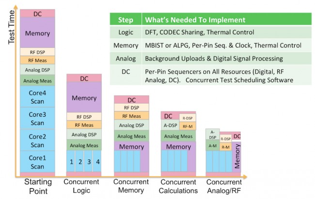
Figure 7 A series of steps necessary to cut test time through increased parallelism (Source: Synopsys)
There are various opportunities for increasing parallelism when testing a complex device, such as the complex multiprocessor mixed-signal device represented in Figure 7. Reading left to right across this figure, the first obvious step is to test the four cores in parallel, which demands the kind of DFT infrastructure discussed earlier in this article, as well as codec sharing and careful thermal control to avoid overheating the device.
The next logical step is to test the memory in parallel with the cores, either by using a memory built-in self test approach, or, if the memory blocks are pinned out, by using an algorithmic pattern generator that can run asynchronously to the rest of the design. Memory testing may need different clock rates when compared to the rest of the design, so the tester will need per-pin clocking and sequencing control, as well as good thermal control. Once the processor cores have been tested, there is an opportunity to use some of the time saved to test the interaction between the cores and the memory, as shown.
Analog and RF tests each demand a different test set-up, so they need to be handled separately. But there is an opportunity to overlap the analog DSP calculations with the RF measurements as concurrent threads, which allows the DC testing to execute as the analog and RF DSP calculations are completing (these calculations can even continue while the tester is indexing to another site). Achieving all this parallelism demands very flexible DC and analog power supplies, and concurrent test-scheduling software to manage the complexity of the approach.
Another way to increase test throughput is to take advantage of increasing tester speeds. It is also possible to speed up scan rates for some parts of the pattern, and slow them down in others, to optimize throughput. Running everything at full speed all the time may not be the most effective approach, especially given the implications of possible branches in the test code. For example, it wouldn’t make sense to allow one part of the test to run at full speed while another concurrent test was stalled, if the end result was to thermally limit the test speed of the whole chip once the stall had cleared.
Managing test branching
Each site in a multisite test will run through the same test logic, being subjected to different tests depending on decisions made at branching points in the test script based on results so far. The overall time to test all the sites will therefore be the sum of the time for each sub-test, plus a little extra for the branch decisions. We can see this in Figure 8 – even if the device at Site 1 passes Test 1and so is effectively finished, it still has to wait for all the other sites to undergo their combination of tests:
Figure 8 Different sites may take different routes through the test script logic, but the overall test time remains the sum of the duration of all the different blocks (source: Advantest)
Advantest’s T2000 tester enables each site to follow its own sequence of tests, in parallel with the other sites. Although this may seem a small distinction, it means that the time to test all the sites becomes the maximum time for any site to take its individual route through the test script, i.e.
TestTime = T1 + Max (T2+T3+T4, T2+T3+T7, T5+T6+T4, T5+T6+T7)
Conclusions
Concurrent and multisite testing strategies make very similar demands on ATE, calling for flexible testers with as much circuitry as possible behind each pin, and the ability to apply these per-pin test resources independently and/or in concert with other pins, as needed.
Tester facilities need to be matched with creative design tools that can facilitate codec sharing and enable concurrent testing of identical blocks, as well as test software tools that can sequence tests to best effect, and a fast-responding thermal-control environment that ensures that devices aren’t damaged by the rate at which they are being tested.
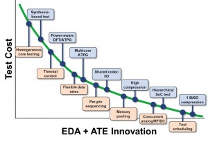
Advances in both EDA software and test systems are “bending the cost curve” down for IC testing (Figure 9). With the right DFT and ATE resources in play, specific cost reduction methodologies can dramatically reduce test time and increase throughput.
Figure 9 How EDA and ATE innovation are changing the economics of test (Source: Synopsys)
Authors
Adam Cron, principal engineer, Synopsys, is part of the test automation implementation R&D group and has been with the company for more than 17 years. A Syracuse University graduate, Cron has worked in test-related fields at Motorola and Texas Instruments for a total of 31 years in the industry. Cron has worked on many IEEE standards efforts, is currently vice-chair of IEEE Std P1838, and is an IEEE Golden Core recipient.
Chris Allsup, marketing manager in Synopsys’ synthesis and test group, has more than 20 years combined experience in IC design, field applications, sales, and marketing. He earned a BSEE degree from UC San Diego and an MBA degree from Santa Clara University. Chris has authored numerous articles and papers on design and test.
Dave Armstrong, director of business development, Advantest, received degrees in electrical, computer and environmental engineering from the University of Michigan in 1974. He has more than 35 years’ experience spanning IC design, product, yield and test engineering, and ATE design, applications engineering and sales. As a principal engineer in Hewlett-Packard’s (and later Agilent’s) IC test group, Armstrong greatly influenced the design and successful market penetration of a long list of ATE solutions. In 2004 he moved to Advantest America, becoming the director of marketing, product engineering, and eventually business development. In this capacity he works with both customers and advantest research and development to define, develop, and deliver creative solutions to the most demanding test challenges. Armstrong also serves as chairman for the International Technology Roadmap for Semiconductors’ test working group.
