Ensuring the reliability of non-volatile memory in SoC designs
This article describes various non-volatile memory (NVM) intellectual property (IP) alternatives with specific reference to their integration within system-on-chip designs targeting the 65nm process node and below. The article considers many of the strengths and vulnerabilities of these IP options, and then describes the tests that must be undertaken to ensure their long-term reliability, particularly for mission-critical applications
Non-volatile memory (NVM) is beginning to occupy more real estate on system-on-chip (SoC) designs in process geometries at and below 65nm.
NVM is essential to store data for trimming analog and mixed-signal cores that require adjustment to compensate for aging effects or for changing operating conditions (e.g., temperature and supply voltages). It is also used to store boot code for on-chip CPUs and DSPs as well as encryption keys used for implementing control of authorization and copy protection in the SoC (e.g., conditional access, high-bandwidth digital content protection and digital transmission content protection).
The consequent proliferation of NVM on SoCs has raised the problem of ensuring the reliability of these elements in designs that contain mission-critical data. Other uses include firmware, program code, configuration code, parametric yield recovery, ROM patching and replacement, and serial Flash or EEPROM replacement.
In the logic space, the more widely used NVM technologies are:
At the 65nm node, embedding floating-gate technology in a logic CMOS process becomes problematic because of short channel effects (SCEs). As channel length decreases, threshold voltage––the voltage required to turn on a transistor––begins to decrease and leakage current increases. This inevitably reduces a cell’s ability to retain data. The problem increases further still at smaller geometries.
Flash suppliers have sought to address the issue by using non-standard process technologies, but this is a far too expensive approach when embedding flash in a standard logic CMOS SoC.
In the case of e-fuse solutions, some fuse material tends to regrow after blowing at a later point in time, again increasing the risk of eventual data loss. Moreover, high current and specific voltage are needed to blow the fuse during programming that require a dedicate SoC pad/pin. Availability, capacity and area vary as e-fuses are usually provided by a foundry and as such depend greatly on how much effort that foundry spent on the design. Foundry supplied e-fuses cannot be used in competing foundry processes, complicating second sourcing supply solutions. On the newer high-k metal gate (HKMG) processes at 28nm and below, the traditional poly fuse can no longer be implemented and is being replaced by a metal fuse.
The anti-fuse solution, such as the memory IP from Kilopass Technology, has advantages over both these alternatives. Foremost among these, anti-fuse is constructed using a standard logic CMOS process. It requires no additional process steps or exceptions to the standard manufacturing flow. That is because at process geometries below 180nm, the gate oxide breakdown (BVox) is less than that of the junction breakdown (BVj).
Therefore, there is no need for a special dielectric or junction implants. As process technology scales, the anti-fuse programming voltage required to break down the gate oxide decreases with transistor dimensions and the oxide thickness. Achieving smaller areas, active and standby power, and higher performance is possible. This results in lower-cost embedded NVM solutions.
NVM test requirements
As with any semiconductor process, NVM integrated into any SoC must pass rigorous stress testing to ensure reliability in the real world. This stress testing makes it possible to replicate failures that may occur over many years of device operation in high volume by using a smaller sample size over a shorter time with accelerated stress applied.
Reliability testing of NVM IP depends on the technology. For fuse technologies offered by foundries and anti-fuse technology, reliability testing includes ‘high temperature operating life’ (HTOL) and process characterization tests such as ‘data retention bake’ (DRB) and ‘high temperature storage life’ (HTSL). For floating charge-based technologies that are multi-time programmable, ‘program/erase endurance’ testing is also required.
Failure mechanisms
Field failures do not occur at a uniform rate, but follow a distribution in time commonly described as a ‘bathtub’ curve (Figure 1). The life of a device can be divided into three periods: ‘early life’, ‘inherent life’ and ‘wearout’.
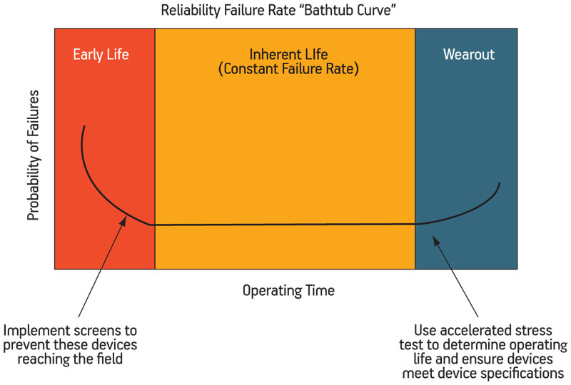
Figure 1
The ‘bathtub curve’ for flash failures. Source: Kilopass Technology
The early life region is when the failure rate progressively improves. The purpose of the test here is to detect and quantify the presence of failure mechanisms that occur in manufacturing as a subset of the device population. Automated test equipment (ATE) screens can be used to prevent these devices from reaching the field.
Inherent life test is designed to detect failure mechanisms intrinsic to all devices in the population. This test provides an estimate of the failure rate beyond the early life period. Results from accelerated conditions are translated to field reliability expressed as FITs (‘failures in time’) of the product.
The wearout region demonstrates a rapidly increasing failure rate. These failures are generally associated with such mechanisms as metal migration or gate oxide breakdown.
HTOL test
HTOL test is performed to determine the reliability of devices under operation at high temperature over an extended period of time. Reliability demands that both 1s and 0s are preserved during the lifetime of the product. The device is powered up and running in functional operation: in the case of an NVM, this means continuously reading from the memory.
The test consists of subjecting the device to a specific voltage bias for a specified amount of time and a specified high temperature, similar to production burn-in. But, unlike burn-in, which accelerates early life or inherent life failure, HTOL is applied to assess the potential operating lifetime of the sample population. HTOL is a long-term burn-in and results provide an estimate of the operating life and field failure rate of a device.
HTOL test checks each region of the ‘bathtub’ curve for functionality. The early life test aims to detect and quantify failures during manufacturing and early in the device’s life due to process manufacturing defects. Readings at 12, 48 and 168 hours during HTOL are taken to determine the early failure rate. The time-to-first failure can be estimated based on the early failure rates. Results from this test help formulate screens that prevent future fallout.
The inherent life test is designed to detect failure mechanisms that are intrinsic to all devices in the population. A reading is taken at 500 hours during HTOL to determine the failure rate. Results from the accelerated conditions are translated to standard application conditions using appropriate data models and activation energies in order to estimate the field reliability of the product in FITs.
A reading at 1,000 hours during high temperature bake is taken to determine the wearout region. In the memory industry, 1,000 hours is equivalent to 10 years of operating life.
High temperature storage life or data retention bake
HTSL or DRB is performed to determine the data integrity of devices at high temperature over an extended period of time.
One of the fundamental requirements of NVM is data retention. An NVM product must guarantee a period over which data will be retained by the device, and is coupled to temperature. In floating charge-based NVM technologies such as flash, data retention is a process of trapping electrons in the storage medium. DRB is used to characterize the ability of the device to retain the appropriate level of charge.
Abnormal levels of charge gain or loss can result in a change in the number of electrons in the stored dielectric medium and, therefore, compromise data integrity. For some NVM technologies, both high and low temperature bakes are required to ensure the charge stored is preserved. In production, it is recommended that a high-temperature wafer bake or final test bake be performed to ensure reliability.
In an oxide breakdown NVM technology, data retention is defined by sustaining the 1s modeled by an equivalent resistor created from the oxide breakdown. HSTL or DRB is used to characterize the ability of the device to sustain the resistor value. The change in the resistive value would alter the current flow to the sense amplifier, compromising data integrity. There is no charge stored in an oxide breakdown NVM technology, so there is no problem with holding the charge.
Program/erase endurance
For flash-based technologies such as floating gate, hundreds of thousands of program/erase cycles are possible. So, the ability to repeatedly program and erase a memory cell, defined as ‘endurance’, is critical. This test is performed to ensure that the memory is able to sustain repeated change in the data state. The most common failing signatures are charge loss/gain issues due to charge trapping or oxide rupturing occurring in the dielectric medium during program/erase cycles.
The endurance test is done at the various operating temperatures for a duration rated by the technology. For logic NVM technologies such as fuse and anti-fuse, which are one time programmable (OTP), endurance testing is not required.
As process geometry continues to shrink and the amount of on-chip non-volatile memory increases, the advantage moves from floating-gate and fuse-based NVM technologies to anti-fuse alternatives. And, the need for exhaustive testing grows in importance for all three versions of NVM.
Andre Hassan is Field Marketing and Applications director at Kilopass. He has over 20 years of semiconductors and systems experience. Hassan has also held senior management and engineering positions at Sigmatel, Monolithic System, S3, Sun Microsystems and Digital Equipment.
Kilopass Technology Inc.
3333 Octavius Dr.
Suite 101
Santa Clara
CA 95054
USA
T: +1 408 980 8808
W: www.kilopass.com
