How to achieve more accurate NAND soft-bit error injection
The article describes a pre-silicon strategy for the design and verification of SSD controllers that is faster and more flexible than ICE using physical NAND on a daughter-card.
As NAND storage technologies and use models evolve, so do the verification tools needed to solve the challenges they present.
In particular, designing SSD controllers targeting NAND flash as the storage media requires some heavy lifting when it comes to dealing with the soft-errors that the flash will eventually produce. A method that simplifies the design and verification of SSD controllers is required.
The soft-bit error function of a TLC NAND device can be imitated by applying a probability mass function to the hard and soft-bit voltage thresholds. These curves can be fit close enough to the real thing to provide a model capable of creating and tuning the BCH/LDPC codes, hardware and firmware functions much earlier in controller development.
By simply setting the mean and standard deviation for each of the probability curves for the TLC device, we can filter the returned data and inject errors according to the probability they will occur per cell. These errors will accurately reflect the physical MSB, CSB, and LSB voltage level relationships.
We model these soft-bit behaviors with an emulator in a virtual setup, which reduces the time to market for the SSD and allows us to build hardware and software both together and earlier.
Modeling NAND behavior
Multi-level cell NAND flash stores a single voltage level on a cell, the analog value of which determines the value of the bits. For TLC NAND, there are three bits possible per cell, or eight voltage levels possible to select per cell.
There are three effects on a NAND that cause the voltage level to shift over time and make it more difficult, or even impossible, to reproduce the correct data:
- Program/erase cycles – these increase the right tails of the probability mass function distribution
- Retention, time, and thermal changes – these increase the left tails of the probability distribution
- Read disturbs
To offset minor voltage perturbations, ECC is used to cover the hard data read. Eventually, however, the ECC cannot correct the data. The first level of recovering the data is to do multiple read-retries. This level is hard-bit reads only, and relies on LDPC (low density parity-check codes) error correction codes in order to recover the data. The second level of recovering the data, and the focus of this article, involves moving the read threshold voltages in the right direction, higher or lower and to the point where the NAND returns at the most likely value.
Hardware may use many discrete levels and a binary search to determine if the actual level is above or below the reference level to find the actual cell voltage. It should be noted that each of these sense operations takes time and impacts performance. Techniques to minimize the latency these operations induce can be created and tested with a model prior to actual silicon. This offers us a great advantage and flexibility to create next-generation controllers within compressed schedules. Controller developers can experiment with configurations for emerging NAND technologies that are not yet available.
When we model a physical process, we are attempting to provide a useful approximation of the physics. The simpler we can do that while maintaining high fidelity, the faster we can simulate and get results as if we were connected to a physical NAND device. Firmware changes and development can be more costly and time-consuming than a hardware change. The goals are fewer firmware changes post-silicon and running firmware much earlier.
We can model this behavior without the complex physics, but complex enough so the model mimics reasonably accurate behavior. Modeling NAND can be simplified and abstracted to a few basic equations and a series of commands. We have found the results to be highly accurate compared to physical NAND, and good enough to develop production-quality firmware much earlier than would be possible with a physical device alone.
Controller companies can do this by extrapolating and curve-fitting the actual data characterized by the vendor, or by themselves. The characterized NAND can be used to tune the model to exact standards, but isn’t necessary to test basic soft-bit functionality (read retries with modified voltage reference matching a distribution function). We can extrapolate enough data to get a reasonably good curve-fit using a distribution, as shown in Equation 1.
Where x is the voltage threshold, and σ and µ are chosen to fit the distribution function to the actual data characterized in the NAND over time. Using this equation, and Microsoft Excel, we now only have to choose where these curves begin and end over time.
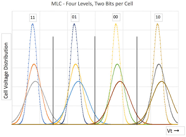
Figure 1 shows an MLC NAND, and four probability mass functions. The far left curve represents the beginning of life of the NAND, with 3,000 cycles (for this particular characterized NAND). Whether the beginning of our TLC part is considered 3,000 cycles or 10, it is the first curve, designated as Bin 1.
The next function (orange line) in Figure 1, represents mid-life of the NAND, or perhaps 20,000 program-erase cycles, where the function is now wider. The grey line in Figure 1 represents end of life of the NAND, or 40,000 cycles, conspicuously overlapping its neighboring function. The equation can be plugged into an Excel spreadsheet to visualize the values for this curve fit.
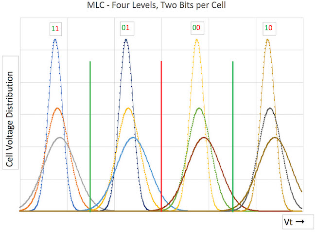
In Figure 2 the distributions shown are for an MLC where first the read reference voltage for the LSB is done (red line), with one read. In order to determine the MSB, two reads are done (green lines). The first read determines whether the programed voltage level is above or below the reference. The next read(s) determine the same, but at different read reference voltages. By doing these subsequent reads, we determine the two-bit value of this MLC cell.
Soft-bit data represents the likelihood of hard-bit data to be accurate. As we expand the range of our soft-bit voltage thresholds, positive and negative, we can find the exact minimum between probability mass function bumps, which is the best hard-bit voltage threshold value possible.
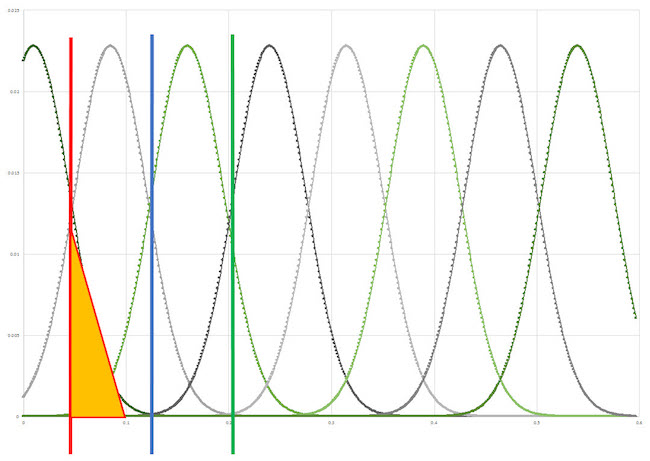
We use an Excel spreadsheet to approximate reasonable curves for a TLC NAND, with seven threshold voltage levels. TLC is just an extension of this same principle with all eight probability distributions for three different ages of NAND, each (Figure 3). As the NAND ages, the peak amplitudes of the functions are much lower and the distribution is wider, overlapping and interfering with each other.
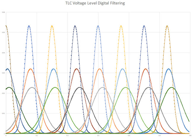
Figure 3. TLC voltage distributions for three different ages of a device, for all eight levels (Mentor)
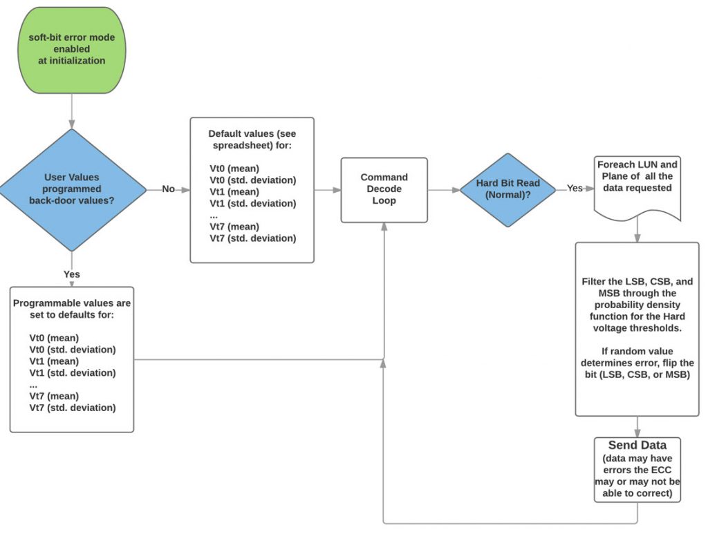
The commands to set these voltages are different for different vendors, but regardless of the commands, the process is the same (see Figure 4). It starts with the initialization and the default parameters for the distribution functions (mean and standard deviation for all eight levels for a TLC NAND). For our purpose, we assume all cells age at the same rate, but in future versions we may track the age of each block. The user can then program different values to set different aging characteristics. The mean will drift upward with age, moving the peak of the curve to higher Vt. The standard deviation will increase (widening and lowering the amplitude peak of the curve).
LSB Example
For all hard-bit reads, the data are filtered through the probability mass function filter for LSB, CSB, and MSB. The value of the actual data (written to the LSB page) is combined with the results of the summation of the Vt0 probability mass function up to the read reference voltage (see Equation 2).
Where Y is the data for the page, Vt0 is the probability mass function, and Vr0 is the hard read reference voltage. The results for each bit in the LSB, CSB, or MSB page, has a probability that the bit will be flipped when returned.
For example, as seen in Figure 5, the red line indicates the read threshold voltage for the 1st LSB read. Consider the case where the programmed level is 0 volts, so that the MSB, CSB, LSB == ‘b111. The actual value of that programmed 0 volts can be anywhere under the first curve on the left. The probability that the CSB == 1 is very high (the blue line indicates Vth for the first CSB read), and so we say that it is 1. The probability the MSB will return a 1 is also very high (the green line indicates Vth for the first MSB read), so we say that it is 1.
That just leaves us with having to calculate the probability of the LSB, which is visualized as the colored area under the curve from 0 to Vth, and is the total probability that the first LSB read will return a 1. In this case, it looks to be about 80%. The orange triangle represents the 20% chance that it will be above the Vth, resulting in an error. So, for this example, if our random number generator between 0 and 1 is between 0.80 and 1.0, we will flip this bit and return a 0, and the whole cell is returned (in error) as ‘b110.
Conclusion
This deterministic (i.e., repeatable) methodology uses the TLC NAND model to initialize and produce accurate soft-bit errors. A device controller can use these soft-bit errors to shift the read threshold voltages to retry the read, and return accurate hard-bit data.
Controller developers gain a powerful tool to explore and develop hardware solutions and software algorithms, pre-silicon. This strategy has been shown to be a faster and more flexible method by which to design and verify a controller versus using physical NAND on a daughter-card running in circuit with the emulator.
Further reading
To take a closer look at the verification and design challenges of NAND technology and for a deeper dive into this solution, please download the whitepaper, Mentor TLC NAND Softmodel Soft-Bit Error Injection

