Towards an infrastructure for profitable DFM
The real objective of design for manufacturability (DFM) is to improve a product’s profitability and manufacturing predictability for its market window and unit volume by optimizing tradeoffs between design costs and manufacturing improvements according to a holistic, lifetime view of the product. Current DFM practice often falls far short of that goal. For instance, the most common design mistake made during the DFM stage is the pursuit of small, incremental improvements in yield that are out of proportion with attendant design costs or schedule delays.
Examples are all too familiar. A design team might blindly follow an arbitrary deck of ‘DFM rules’ that lack the confirmation of quantified and up-to-date models and process data. Resulting errors cost millions of dollars attributable to slipped schedules, yield problems, and/or poor performance. Alternatively, a ‘recommended rule’ might demand redundant contacts in every cell and redundant vias on every route, even though these can actually decrease overall yield because they increase the chip’s critical area and lead to higher leakage surrounding every gate.
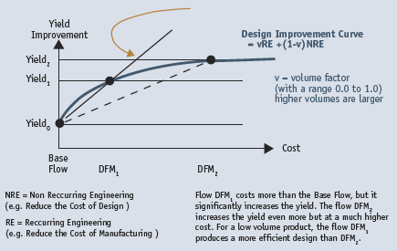
Figure 1. The most efficient design has the maximum slope and not the highest yield
To move beyond such local optimization practices, this paper proposes a DFM infrastructure now being developed under the banner of the DFM Coalition (DFMC) and through the well-established Silicon Integration Initiative (Si2). It gives designers the ability to make reasonable tradeoffs between design and manufacturing costs for a given unit volume while meeting targets for tape-out, chip size, density, performance, and power (Figure 1).
Reaching the limits of light and lenses
Until the 65nm process node, each technology generation was accompanied by both a reduction in the wavelength of light and an increase in the numerical aperture of the stepper/scanner used during lithography. Lithography requires an extremely tight phase control of light as it exposes the wafer’s resist to define circuit features. Waves of light that are in-phase enhance each other; out-of-phase waves can cancel out each other to the point where exposure does not occur. Lenses that worked well at wavelengths above 197nm began to exhibit two indices of refraction, called birefringence, when pushed to smaller wavelengths. Researchers found that as they developed lithography technology using 157nm light, light waves could enter a lens inphase but come out slightly out-of-phase resulting in destructive interference. The tight phase control required for exposing the resist had been lost.
Traditionally, lenses had grown in size with larger numerical apertures to provide higher resolution. However at 65nm and below, some scanners began to use immersion lithography, employing a liquid between the lens and the wafer to increase the numerical aperture. Thus, manufacturing yield became limited by systematic effects such as process window lithography and the on-chip variability of circuit parameters.
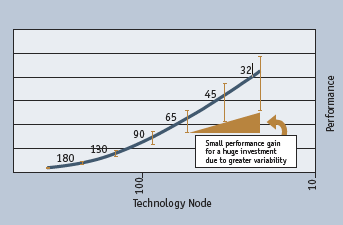
Figure 2. Parametric variability

Figure 3. Exponential rise of DRC rules
The expected performance gains usually accompanied by moving to a new technology node were diminished because the worst cases for a chip’s parameters covered a larger range than for previous nodes (Figure 2), forcing engineers to make more conservative design assumptions. This then led to sub-optimal performance goals.
Because we are reaching the limits of light and lenses, quantified DFM models are required to inform chip designers which patterns have greater fidelity across the process window and which cell layouts have less parametric variability, and thus greater predictability in product performance.
Diminishing returns from doing more of the same
The total number of design rule checks (DRC) for physical design has more than doubled over the last three process generations (Figure 3). DRC rule decks now contain over 1,500 rules that must pass prior to DRC signoff. The most recent 1,000 DRC rules were added at sub-100nm process nodes due to the inherent limitations of deep sub-wavelength lithography.While the first 500 DRC rules clearly described the primary layout constraints, those last 1,000 are more complex and harder to follow since they describe a growing variety of ‘corner case patterns’ that require ever more specialized layout rules and represent highly non-linear physics effects.
Today, the move from a rule-based view of physical design to a model-based view gives designers the ability to quantify economic tradeoffs between design and manufacturing. A few hundred DRC rules accompanied by a mere handful of accurate models for lithography, critical area, chemical-mechanical polishing and stress provide better feedback to designers than thousands of DRC rules in isolation.
Recommended rules or recommended patterns?
There is growing controversy over the usefulness of ‘recommended rules’ during DFM. One keynote speaker at ICCAD 2007 claimed that “80% to 90% of recommended rules are worthless”. Several leading DFM researchers are now advocating a layout methodology that instead promotes ‘recommended patterns’. Restricted design rules (RDRs, Figure 4) enforce a layout composed of a limited number of regular and well-characterized layout patterns. Defining a small set of recommended patterns – as opposed to a large set of patterns requiring specialized rules – is a more efficient way of getting designs into early production at new technology nodes and quickly ramping up the yield curve. RDRs focus on optimizing manufacturability through techniques such as aligning all transistors with a common orientation using only the preferred poly pitch. Interconnect routing is also very regular, with greater uniformity in metal density to minimize problems during CMP.

Figure 4. Restricted design rules
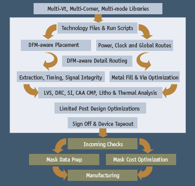
Figure 5.The interplay of elements in the DFM flow
Use of recommended patterns rather than recommend rules can manage problematic patterns at route corners, avoiding bridging and necking at the edges of the lithographic process window. An intelligent use of redundant vias and a greater overlap of the metal around the vias make designs less prone to single via failures or misalignments of metal and via.
While foundries are likely to revise recommended rules, lowering their priority or even removing them as a process matures, recommended patterns are likely to remain intact since they become part of the library and design ecosystem. Additional patterns that save area for certain layout styles can then be added as a process matures, but their addition will not invalidate the original cell layouts.
Increasing the dimensions of design optimization
A good DFM infrastructure must bridge the information islands in design and manufacturing by supporting various collections of EDA tools that share information and design tradeoffs between each other. Legacy EDA point tools were often totalitarian systems that did not readily share information or work collaboratively with other tools.Worse still, the tool interfaces were designed to ward off the competition, thus preventing the lossless translation of data between successive tools from different vendors coexisting in a user’s flow. A few design tradeoffs were made in each point tool and every point tool greedily consumed any timing or area slack in the design for itself. It was common for an implementation (e.g., place & route) tool to conclude that it met timing, power, signal integrity, and routing constraints while obeying complex design rules, yet a downstream analysis would find hundreds or even thousands of timing and/or DRC problems. These problems had to be fixed manually or sent back to P&R via engineering change orders that reworked a design, only to fix some problems and introduce some new ones.
Today, contending metrics derived from timing, power and signal integrity constraints are forcing changes to design methodologies. The old ‘command and control’ structure of point tools in a sequential design chain is giving way to a hub of tools that share information and conduct profitable transactions via the DFM infrastructure to optimize the design. DFM is a new and compelling force that is driving these changes further and faster than ever before. Communication and collaboration between tools via standard protocols provides a deeper insight into a wider set of design information than any single point tool could previously acquire (Figure 5).
Modern DFM-aware placers and global routers now communicate to support voltage islands,multi-corner/multi-mode analysis, buffer insertion, buffer resizing, gated clocks, cloning clock networks, and cross-library optimization that substitutes lower power or higher yielding cells into the placement.Modern DFM-aware detail routers now communicate with specialized tools for 2.5D parasitic extraction, wide-wire spacing, line-end spacing, wire spreading, redundant vias, and shielding and spacing for signal integrity.
Why will companies co-operate on a DFM infrastructure?
Open community standards allow companies to focus on building their differentiated applications on top of an infrastructure of transparent source code. This source code, implementing the standard in a practical and adoptable manner, can then be supported by a larger community of experts than any single company could ever afford to hire (assuming they could attract them in the first place).Matching this truism to the desired DFM infrastructure will allow the resulting infrastructure to leverage the combined knowledge of industry experts and thus provide the most compelling and functionally robust solution.
Examples of successful open community standards, such as OpenAccess, are not just good open standards. These technologies are cited as ‘best-in-class’ standards that users find significantly better than the systems they replace. Since input for such standards comes from a wide variety of perspectives, the final system is more flexible and comprehensive than a system completely specified within a single company. These standards are also created in a process that prevents forking, thus promoting greater market acceptance and preventing market confusion.
Standards also enhance the movement and reproduction of best practices learned from other members, which further aids innovation. As an example, within the DFMC at Si2, it was a common practice for some members to place design intent tags on cells and wires, but a totally new concept to a few others. Those who had not taken this approach quickly recognized its value and produced sets of tags customized for their own design flows.
Conclusion
The time is right for the industry to develop a DFM infrastructure that will support more thorough and interoperable data communications, enabling profitable transactions between design and manufacturing that achieve the need for global optimization.
The goals of Si2 and the members of the DFMC is to build open standards that realize this vision and then ensure that it can be quickly and safely adopted. It is critical to provide a safe legal framework that protects both the companies that collaborate on a standard and the end-users who adopt that standard.
Adoption of these open standards will lower the barrier to innovation and promote the acceptance of tools from startups. It will drive greater integration of best-in-class design capabilities from a variety of suppliers.
Silicon Integration Initiative
9111 Jollyville Road, Suite 250
Austin
Texas 78759
USA
T: +1 512 342 2244
W: www.si2.org