The waiting game
As part of our nanotechnology focus, we look at the prospects for graphene and carbon nanotubes in electronics. Paul Dempsey reports.
Graphene. It’s a big deal. It has to be because it was the subject of the 2010 Nobel Prize. And the prizewinners, University of Manchester scientists Andre Geim and Konstantin Novoselov, have indeed been pioneers in taking our understanding of this carbon allotrope to ever higher levels. Yet Geim himself has long been cautious about how long it will take for us to see advanced electronics applications, referring a little wearily to the idea of “Graphenium Inside.”
For starters, in its normal state, graphene has no bandgap—and that effectively rules out even its medium-term use in digital circuitry, where a fairly sizeable bandgap is necessary for a high current on/off ratio. That said, for analog and optoelectronic communications things could happen sooner.
Graphene has properties that could help it turbo-boost chips used in the RF and microwave domains. Already, the US military is putting serious funding into research for that type of application through the CERA (Carbon Electronics for RF Applications) program run by the Defense Advanced Research Projects Agency (DARPA).
There is, however, a need to separate hype from reality. Even the most successful researchers emphasize that work is very much at an early stage. Techniques to create basic graphene field effect transistors (FETs) in the lab have been demonstrated using variations of mainstay CMOS semiconductor manufacturing processes, most notably by IBM (Figure 1). But while the results are promising, they are also some way short of mass production.
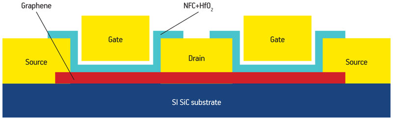
Figure 1
IBM’s proposed graphene FET
The general consensus is that graphene-based chips are unlikely to be seen in volume until semiconductors reach the 6nm process node, currently foreseen on the ITRS roadmap for 2024. Nevertheless, when graphene then starts delivering its potential, it could be a real game changer.
In simple terms, graphene is made up of a two-dimensional, one-atom thick hexagonal lattice of carbon atoms, usually described as resembling chicken wire.
For communications, its most valuable property is its high carrier mobility: electrons can theoretically move through it at a staggering 200,000cm2V-1s-1 (silicon has mobility of around 1,400cm2V-1s-1). It then also boasts constant optical absorption over a wide range from far infrared to near ultraviolet, and strong thermal and mechanical performance. Today, though, that potential mobility number seems a distant target.
At the recent International Electron Devices Meeting (IEDM), Phaedon Avouris, an IBM fellow and lead of its Nanoscale Science and Technology Group, said that his company has fabricated graphene FETs on a silicon carbide wafer with a cut-off frequency of 170GHz for a drain voltage of 2.2V. The comparable cut-off frequency for present-day devices is around 40GHz. The work followed on from IBM’s achievement of a 100GHz cut-off frequency only a few months earlier.
In addition to the performance range, the other big advance here is IBM’s success in forming the graphene by heating SiC CMOS-compatible wafers to 1,450°C. So far, devices have been made from separately produced graphene flakes and the material’s quality has been highly variable. At the same time, graphene has a more planar structure than carbon nanotubes and that makes its integration into CMOS processes easier.
Nevertheless, as Avouris explained, once you get the graphene on the wafer, what follows is still a tricky process. “To [then] fabricate RF transistors, this continuous graphene layer is patterned by oxygen plasma etching to electrically isolate the channel region, and source/drain electrodes are deposited by thermal metal evaporation,” he said. “Top-gate stacks are then formed by either depositing an organic seed layer (a nanofibrillated cellulose polymer) followed by hafnium dioxide or aluminum oxide atomic layer deposition, or by plasma-enhanced chemical vapor deposition of a thin silicon nitride film followed by a gate metal deposition.” The graphene FETs were also fabricated using electron beam lithography, another CMOS-compatible technique.
The challenges ahead for IBM lie partly in the fact that while the achieved hole mobility—at around 1,500 cm2V-1s-1—is high relative to the state-of-play, it is still some way short of graphene’s potential. Similarly, the effective gate length for the transistors was comparatively large at 90nm, although a notable advance on the 240nm reported in 2010’s first announcement from the Avouris group.
He said that the group sees the next step as the application of a self-aligned gate fabrication technique that IBM has been developing. Using that, he added: “We estimate that the RF performance and the cut-off frequency can be enhanced by a factor of two.”
This is groundbreaking work but also very much in the pathfinder mode. And so much is even truer of research under way in optoelectronics, where IBM is also pursuing graphene technology.
As for digital circuitry, the initial challenge in using graphene here is the ‘natural’ absence of a bandgap. However, for optoelectronics, there may be a way forward if a comparatively smaller one than that needed for, say, a microprocessor can be induced. Avouris said his team has developed the basics for such a technique.
“One way to create a bandgap involves the application of a strong perpendicular electric field to AB-stacked, bilayer graphene. These bilayers have a four-atom unit cell, hyperbolic dispersion and no intrinsic bandgap. The low energy bilayer bandstructure involves two valence and two conduction bands,” he explained.
“The field produces an asymmetry by inducing charge transfer between the layers. The two atoms in the bilayer unit cell that lie directly over each other are rather strongly coupled, so the resulting charge-transfer breaks the inversion symmetry and opens a bandgap.”
So far, this approach has been used to open bandgaps of 130meV and on/off ratios of 100 for room temperature and 1,000 for low temperatures. These metrics could, Avouris said, support such applications as terahertz emitters and detectors. More importantly, he sees scope to improve both the quality of the graphene itself and the dielectric that could bring bandgaps in the region of 400meV, suggesting still wider optoelectronics applications and perhaps paving the way for use in digital chips.
Throughout this work—and other papers that are starting to emerge—runs the message that graphene has passed the proof-of-concept stage. By working from the basis of existing manufacturing techniques, IBM is showing that the semiconductor industry, and its markets for both wireless and wired communications, could ultimately transition to graphene-based designs. But it is also still the case that this is research. Processes are changing all the time and, as with so much in nanotechnology, materials science also looks set to play an important role.
Some devices may emerge before 2024. The relatively small runs required for advanced military communications may mean that chips are produced on a custom basis before the 6nm node. The role DARPA is playing here in seeding and encouraging research would suggest as much, and there are suggestions that military uses could look viable once devices can be made with gate lengths of less than 50nm, where performance is the overwhelming driver. IBM’s success in reducing gate lengths so far may mean this point is reached relatively soon, although for the broader market other metrics and parts of the design infrastructure do need to be addressed.
Also at IEDM, Terry Ma, vice president of engineering at design software vendor Synopsys, noted: “In the longer term, emerging materials and technologies such as graphene and spintronics, which are being considered as possible replacements for CMOS, may require new approaches to modeling such as quantum transport and ab initio methods.”
There is still much to do, often from the ground up, and the reality for graphene is that its wider use in transistors probably lies more than a decade away.
Carbon nanotubes as interconnects
There is a growing range of nanotechnology-based materials that chip designers would like to insert into existing CMOS processes, if possible, as existing options become harder and harder to use.
One such switch is being mooted between today’s copper interconnects and a new generation formed of carbon nanotubes (CNTs). The current density of CNTs can theoretically reach 108 A/cm2, three orders of magnitude greater than that of copper. As chip feature sizes shrink, the potential here is obvious. Moreover, CNTs also potentially offer five times greater thermal conductivity and ballistic electron transport so their resistance is independent of length.
The problem to date has been growing CNTs in the densities and clusters that will be required to reach these levels of performance. Those numbers assume highly parallel tube growth. Beyond that, there is the challenge of forming the CNTs within current semiconductor design structures and processes, using chip-friendly materials.
A team from France’s CEA Leti research think tank, Switzerland’s Ecole Polytechnique Federale Lausanne, and the Engineering Department at The University of Cambridge, is developing such a technique for depositing and growing CNT interconnects with far greater density and capacity than previously seen.
The CNT formation process, developed by Cambridge’s Professor John Robertson and Santiago Esconjauregui, involves generating root growth on traditional conductive substrates (polysilicon for connections to transistors and metal lines for interconnects). Growth is achieved by depositing a thin catalyst—here iron—and changing that catalyst’s properties during heat during annealing to control the CNTs.
The Cambridge approach uses multiple cycles of deposition and annealing to maximize spatial density—critical to achieving the kind of transport performance required for minutely featured next-generation chips. It also uses liquid evaporation to achieve densification of vertical CNT structures. The work has produced densities five times greater than those seen for CNTs as vias for electronics to date, although still short of those sought in the official chip roadmap from the ITRS. So far, the team has integrated 2.5.1012cm2 CNTs in 1um diameter vias. The ITRS target is 3.1013cm2.
Nevertheless, an audience at the International Electron Devices Meeting was nearly universal in its praise for the work and, more importantly, its promise. Cambridge’s Professor Robertson is confident that the necessary increases in density can be achieved—and he’s not alone. One of the companies following the work very closely is Intel, the world’s largest chipmaker.