Winning at Whac-a-Mole: redesigning an RF transceiver
A team from RFMD describes a design upgrade for one of the company’s devices, the ML5800 transceiver. The chip is used in cordless telephones and has sold more than 20 million units. Because of constraints upon the different portions of the project and a wish to maximize reuse from the earlier chip, the company developed a new methodology using system-level simulation for the digital circuitry alongside its existing mixed-signal simulation software. The chip uses a two-port frequency shift keyed modulator, a relatively recent technology that enables precise modulation without encountering power amplifier pulling effects. It is one of the reasons for the success of the ML5800, but the more complicated circuitry the feature entails also made it hard to redesign the chip for new applications. For the revised device, the challenge was to increase the data rate from 1.5Mbit/s to 4Mbit/s, so that its market reach could be extended from audio applications to video applications.
In the popular arcade game, Whac-a-Mole, you bash plastic moles on the head as quickly as possible. As soon as you hit one mole, another one pops up on another part of the game machine (Figure 1). Designing a transceiver is much the same, except the stakes are far higher. You have to hit all of the moles before your time and money run out, but now you are up against the best players in the world in a winner-takes-all tournament.
Figure 1
A Whac-a-Mole machine. Source: Creative Engineering
At RFMD, we have learned a lot about the mixed-signal business since our formation in 1991. We are a global company with more than 4,000 employees, supplying RF components for a wide variety of end-uses, ranging from cell phone handsets to cable TV tuners to wireless networks. These are highly competitive markets where vendors are continuously introducing new devices. To stay ahead of the pack, we need to keep offering new devices of our own with advanced capabilities.
One project we have just completed provides a good illustration of how we are maintaining a leadership position through design process innovation.
Measure twice, cut once
We wanted to produce a faster version of our popular ML5800 transceiver, a device that has sold more than 20 million units (1). It is a high-integration, 5.8GHz frequency shift keyed (FSK) transceiver that integrates all the frequency generation, receive and transmit functions required to realize a digital cordless telephone or similar device.
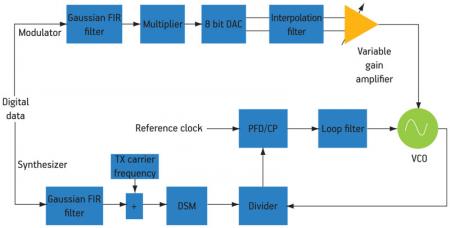
The chip uses a two-port GFSK modulator, a relatively recent technology that enables precise modulation without encountering the power amplifier pulling effects from which other designs suffer (2). It is one of the reasons for the success of the ML5800, but the more complicated circuitry the feature entails makes it harder for us to redesign the chip for new applications. Figure 2 is a block diagram for the modulator part of the ML5800.
Figure 2
Two-port GFSK modulator. Source: RFMD
For the new device, the challenge was to increase the GFSK data rate from 1.5Mbit/s to 4Mbit/s, going from audio applications to video applications. A complete chip redesign would cost more than $4M, so we wanted to reuse as much of the previous design as we could, minimizing design changes and thereby project risk.
Foundry production processes are highly complex, involving multiple interacting layers. Changing these layers means changing the mask set, incurring greater costs and risks across a project. The challenge was to reuse as much of our previous design as possible, making minimal (if any) changes to the mask set. This meant no changes to transistors and limited changes to resistors.
With specific regard to the design process, this translated into changes to filter coefficients but not to the types of filters or even the number of filter coefficients. We wanted to change just the modulation path into our VCO (the top row of the block diagram in Figure 2).
Figure 2
Two-port GFSK modulator. Source: RFMD
Like everyone else, we produce test chips before starting mass production. This is a necessary evil—you need to prove that the redesign works, even though test chips are expensive and time-consuming. Getting it wrong means a respin and too many respins will blow the budget, miss the market window, and see you lose to the competition. So, we use extensive simulation to eliminate as many problems as possible before producing the test chips.
The new device presented a highly constrained design problem for us; we had very limited parameters we could alter. The trouble was that changing one part of the system affected other parts. We would get one part of the system working well, say the analog part, but then would run simulations and find that the digital part had popped out of specification, and vice versa—just like Whac-a-Mole. The challenge in playing the game this way is our design process; we optimized it for accuracy, not for quickly iterating through design alternatives.
Slow and traditional
Traditional mixed-signal chip design relies on very low-level, detailed device simulations using languages like Verilog for the digital portion, and SPICE for the analog portion. These simulations very accurately predict the behavior of the real device, but are very time-consuming to run.
The problem presented by slow simulation times is compounded by the verification process for mixed-signal behavior. Typically, you will run a simulation of the digital part of a system, export the results to a data file and read that file into an analog simulator. In turn, you will run an analog simulation and export the results into a data file, which the digital simulator reads. This process is slow, awkward and very, very painful.
Mixed-signal design involves multiple iterations. You try something; you get it wrong; you try something else. You get closer and closer to the solution. Each design iteration means rebuilding the Verilog and SPICE models and running slow simulations.
Meanwhile, these models are just too detailed for fast design iterations. In our highly constrained design, we wanted to evaluate multiple alternatives and do so quickly. We were looking for a quick way to build and evaluate mixed-signal options.
System-level design seemed like a solution to this challenge. Looking at the literature, we found that the concept attracts varying definitions, so we let our internal requirements determine how we would deploy the concept. We had three basic needs: analog and digital design abstractions, analog and digital in the same model, and co-simulation.
Design abstractions have been available in the digital world for some time, taking engineers away from circuit elements and parasitics into the abstract world of logical system description. These abstract digital descriptions enable engineers to build systems very efficiently. We wanted something similar for the analog parts of our designs.
A more abstract analog model reduces simulation fidelity, but the benefit is much faster simulation. The ideal use case for us is to use abstract simulation to find a ballpark solution, and then use detailed low-level simulation to reach our final solution.
We design mixed-signal transceivers, which means we have analog and digital components in the same device. We want to simulate our complete analog-digital device in one simulation environment. We also want to avoid the very painful verification process that results from using separate tools. Simulating analog components in an analog design tool and digital components in a separate digital tool, does not really allow you to study and understand the behavior of the system as a whole.
You cannot just flush away existing tools and models. They represent a substantial investment, and in our case, we know they are very accurate, if slow. We had trusted Verilog and SPICE models for the ML5800 transceiver and we wanted to use them in our new device design process. Our system-level design process therefore had to link into the existing design infrastructure.
Going faster through abstraction
The team tried different system-level design tools. Most of them offered digital simulation, but a smaller number offered both analog and digital simulation. When we looked at ease of integration with our existing tools, we decided to work with MathWorks Simulink (3). It was particularly important to us that our system-level tool linked to our analog tool, Virtuoso Spectre from Cadence Design Systems (4), because we have a great deal of intellectual property wrapped up in Spectre models.
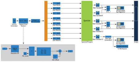
Spectre links to Simulink with ‘couplers’, which appear as blocks within the two simulators. To use co-simulation, we constructed a model and used these blocks where we wanted to couple to the other simulator. Figure 3 (p. 41) shows one of our Simulink models, with the Spectre co-simulation coupler block.
Figure 3
Simulink-Spectre co-simulation via coupler blocks. Source: RFMD
At the start of the design process, we did not know if we would have to change the analog, digital, or both parts of the ML5800 design. We knew we wanted to retain the basic structures of the digital filter, multiplier, DAC, interpolation filter and variable gain amplifier. This left the filter coefficients in the FIR filter, interpolation filter and variable gain amplifier.
To add to the challenge, design constraints meant we could not change the clock frequency, so the higher data rate target of 4Mbit/s meant reducing the number of samples per symbol, making the task of the interpolation filter much harder. Changing filter coefficients to increase the cut-off frequency introduces quantization noise and distortion, but we had to stay within design specifications for these parameters. At the start of our design process, we did not know if we would have to change our digital design too. In fact, we did not know if it was possible to get the results we wanted from such constrained design choices—would it even be possible to increase the data rate to 4Mbit/s and stay within our system specification?
The constraints forced us to undertake many design iterations, using different filter settings and evaluating their performance. Our initial guess was that changes would occur mostly to the analog filter settings, so we built a rapid design process based on that assumption.
We created a digital model of the system in Simulink and combined it with an analog model in Spectre. The Spectre model reused our previous analog designs for the ML5800. The combination gave us the benefits of Simulink’s speed for the digital portion of the system, and Spectre’s detail for the analog simulation. The approach was something of a hybrid between true system-level design and more detailed circuit design, but it enabled us to make the limited changes we needed to for this project, and simulate them with the appropriate accuracy and speed.
Our design process was straightforward. We made changes to the analog filter coefficients in Spectre and ran a Spectre-only simulation to verify that the analog portion of the system gave the expected results. Next, we ran an analog-digital system-level simulation in Simulink, co-simulating with Spectre. At the system level, we examined properties, such as distortion, to check that the system as a whole was within specification. We also checked that the candidate design was realizable on silicon—for example, not all amplifier gains are allowed.
As you might expect, our early iterations all failed. We would find that distortion was out of range, or there was some undesirable system-level behavior. It is important not just to know that a candidate design is not suitable, but also why its failure occurred. Our system-level approach meant we could look more closely at the analog-digital interface and gain a deeper understanding of why the system as a whole behaved in the way that it did. Armed with this knowledge, we were able to start the next design iteration from a better place. Figure 4 (p. 42) shows a typical set of results from Simulink, Spectre and the chip itself.
Figure 4
Simulink-Spectre results. Source: RFMD
After several design iterations, we found a design that worked well within specification. About 80% of our effort had gone into changing the interpolation filter, and about 20% into changing the filter parameters of the variable gain amplifier, but we also found that we needed to change the value of the multiplier in the digital scaler after the FIR filter. It was a question of finding which analog and digital gain settings gave us the behavior we needed.
At the end, we found that our Simulink-Spectre co-simulation results were within our specifications. In fact, we had so much faith in our results that we were able to skip detailed low-level simulations required in our previous methodology. The team produced a test chip based on the results of the Simulink-Spectre simulations alone. Bearing in mind the cost of failure, this was a huge endorsement of our new system-level design process.
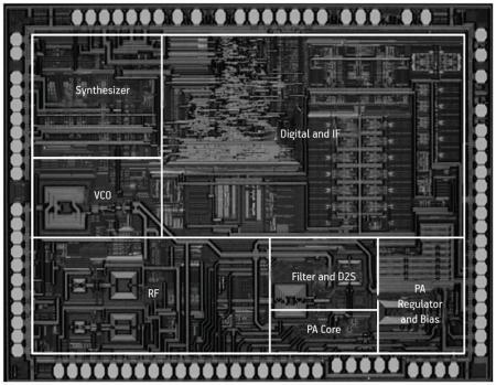
We taped out our design in September 2009. Figure 5 (p. 43) is a die photograph of our transceiver.
Figure 5
Die photograph of the revised transceiver. Source: RFMD
Better by design
Through system-level design and co-simulation, our team produced a working solution in a fraction of the time and cost it would have taken using our previous methodology. The redesign work took six weeks—a very short amount of time for such a highly constrained project.
System-level design means we can make and evaluate design changes very rapidly. Any kind of architectural changes can take a considerable time to evaluate using a lower-level methodology based on Verilog, for example. A lower-level methodology means that all alternatives have to be hand coded before you can evaluate them, a costly process that limits the range of architectures you can explore. System-level design gives you the freedom to quickly explore and evaluate alternatives.
This chip was something of a proof-of-concept exercise. We used the project to work out kinks in our design process for a highly constrained problem. We have been very pleased with our results to the extent that we are using the resulting methodology for more complex designs. System-level design is now an integral part of our design flow.
The new methodology has also strengthened the team. We now have analog and digital people working together using system-level design. We still find problems, but we can deal with them quickly. It’s still Whac-a-Mole, but Whac-a-Mole as a team sport.
References
- ML5800 Transceiver Data Sheet, http://www.rfmd.com/CS/Documents/ML5800DS.pdf
- “A two-port GFSK direct modulator for wideband applications at 5.8 GHz.” Farahvash S., Queek C., Roberts W., Walker D., Mostafa M., Liem H., Koupal R. pp 2128 – 2131, ISCAS 2007
- Simulink web page, www.mathworks.com/products/simulink/
- Cadence Virtuoso Spectre data sheet, www.cadence.com/rl/Resources/datasheets/virtuoso_mmsim.pdf#page=5
RFMD, LLC
7628 Thorndike Road
Greensboro
NC 27409-9421
USA
T: 1 336 664 1233
W: www.rfmd.com


