TrustMe-ViP: trusted personal devices virtual prototyping
As the market continues to push for higher performance at lower cost, trusted personal devices (TPDs) must also be able to exchange greater volumes of data, voice or streaming video at ever higher bit rates, while transmitting and receiving securely under multiple telecommunication standards. Reductions in cost and time-to-market can only be achieved by integrating the complete system design including such aspects as the antenna and the packaging.
The TrustMe-ViP project is part of a larger CIM-PACA (Centre Intégré de Microélectronique Provence Alpes Côte d’Azur) initiative that has developed a virtual RF system-level design platform, and it is specifically dedicated to the design of complex TPD systems. It provides a unified EDA framework that features multiple simulation engines based around dedicated hierarchical model libraries available for multiple levels of abstraction.
The benefits and structure of this methodology are described here and illustrated by way of the example of a Bluetooth transceiver design.
Introduction
Like all electronic products, trusted personal devices (TPDs) have to be more and more competitive, delivering higher performance at lower cost. Reducing the bill of materials and time-to-market can best be achieved through the broadest and most complete integration, one that also includes elements such as the antenna and/or the packaging where smart cards or system-in-package (SiP) technologies are involved. This paper proceeds from the position that designing such complex systems requires the development of a single EDA framework composed of multi-engine simulators that are associated with a library of hierarchical models.
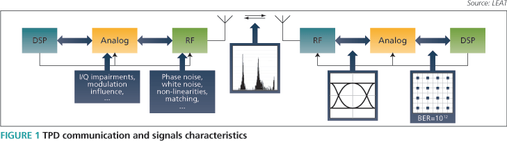
Figure 1 shows the different parts in a TPD and the different types of signal involved in a typical communication between two such devices. It is clear that preparing them to handle the different signal shapes and frequencies is no trivial task. Indeed, during different design phases, engineers have to account for such factors as bit error rate (BER) on one hand, and power consumption on the other. Block design requires that electrical properties are set with due consideration for factors such as noise, nonlinearity, gain or impedance matching. Each step requires different simulators, and all must be interoperable. Even then, there is usually a design gap between the system specification and the RF block design. It typically centers on:
- the use of different design frameworks and different simulators; and
- a huge frequency ratio between the RF (GHz) and the digital baseband (MHz).
Nevertheless, to meet an original system-level specification, engineers need to mix different levels of abstraction so that they can explore implementation architectures and then validate the final design at the circuit level. Luckily, existing behavioral models in the VHDL-AMS analog and mixed signal language provide the basis for such a seamless system-to-transistor-level approach. Relevant features include:
- top-level functional simulations for architecture validation using a top-down methodology;
- bottom-up verification with accurately characterized models;
- test program development using tester resource models;
- traditional measurement, post-processing and/or the use of testbenches; and
- IP exchange and protection to help assess a model against a specification.
This paper describes a methodology for the design of TPDs that can interface to multiple terminals and networks. This methodology is based on the Mentor Graphics’ ADVanceMS (ADMS) framework [1], Matlab/Simulink from The Mathworks, and a hierarchical analog and mixed-signal intellectual property (AMS-IP) library.
The virtual RF system platform
The virtual platform
The different parts of a complex embedded system are usually specified and designed separately by engineers working with various EDA tools. For TPDs and similar communications devices, one must account for critical design parameters (e.g., cost, power consumption, channel effects) at the system level. The exploration and evaluation of various system architectures then requires access to a complete, hierarchical AMS-IP model library and a design environment that supports the use of several design levels. Then, test vectors that have been initially applied at the system level should also be available for reuse at each subsequent level in the design flow.
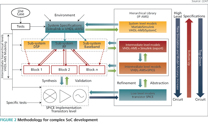
Simulation time is very important. To control its influence on time-to-market, this methodology uses a four-level hierarchical model library (Figure 2): transistor (SPICE or physical level), structural (low level), behavioral (intermediate) and high level (ESL or specification). It is also tailored to the three main types of design process: bottom-up, top-down and meet-in-the-middle [2]. The overarching goal is to define the primitive components and objects, and to then develop them and the system structure simultaneously, so that the final system is constructed from these primitives in the middle of the design process. The same paradigm is used to develop the hierarchical models.
SystemC is used to provide a fast, high-level, C++ based framework for the simulation and to validate the system specifications [3]. Meanwhile, for non-electrical devices (e.g., micro-electromechanical systems [4], photonic components, etc.) finite element methods (FEMs) provide golden simulations [5] at the physical level, in the same way as SPICE does for electronic circuits. These simulations are used to validate a higher-level model or to develop them. In fact, both top-down and bottom-up approaches are suitable in that the hierarchical library can be built by refinement or abstraction.
Limitations of the methodology
The main limitation concerns the development of the hierarchical library. Model development is difficult and needs a high level of expertise to be carried out effectively. Achieving an accurate RF implementation demands the full consideration of such factors as non-linearity effects, compression, noise, phase noise, frequency response, mismatch and so on. Moreover, RF designers also often use proprietary models during simulation, and this often means that there are limited opportunities for their reuse across different design environments.
The problem of coupling by the substrate or the wires must also be considered. Increased digital signal processing (DSP) lowers the quality of analog signal processing. Luckily, mixed-signal simulation is now a mature technology, and several unified simulators and co-simulation solutions are available [6]. This smoothes our path to the objective that, wherever possible, one should reuse existing models and unify various platforms in ways that are transparent to the user. The key factors for success are:
- the ability to take a hybrid approach to the integration of different tools;
- the use of open databases using standard languages; and
- the availability of standard, compatible input/output formats and interfaces.
Tool flow
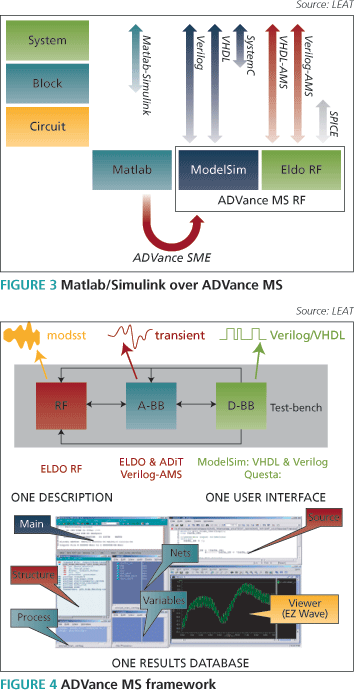
As noted earlier, the platform is based on the ADMS framework coupled with Matlab/Simulink. The main idea is to reuse models developed under Simulink, which offers an RF system baseband modeling simulation where the number of simulation steps is significantly reduced, as well as Simulink user-defined continuous models.
For example, in a Bluetooth [7] transceiver, the wireless system transmits a GFSK-modulated signal at 1Mb/s, using a frequency-hopping algorithm over 79 1MHz sub-carrier channels, with a center frequency around 2.4GHz. In this case, the established models only take into account the spectral peaks within a bandwidth around the carrier frequency. As a result, the first important drawback is the loss of simulated nonlinear behavior outside the bandwidth. A second is a limitation to the modulated steady state (MODSST) simulation. It requires the development of Simulink continuous models because the tool lacks appropriate baseband models. So, for behavioral and functional approaches, we need to run different RF simulations to analyze the complete system. The solution is to export and compile the Simulink models in ADMS, using the Real Time Workshop (RTW) toolbox [8] (Figure 3).
Simulink is a graphical ‘what-you-see-is-what-you-get’ editor based on the Matlab engine. This simulator covers the system level, delivering its results easily and quickly. It allows the simulation of complete transmission systems, including both the digital and analog elements. The simulation accuracy is admittedly limited for the analog portion, but that is counterbalanced by the tool’s system approach to verification and validation. Simulink has thus become a standard language by default, particularly for system-level designers.
VHDL-AMS (or Verilog-AMS) is used to describe the digital, analog and RF behavior. The ADMS framework can cope with mixtures of different languages (e.g., SystemC, VHDL, Verilog, VHDL-AMS, Verilog-AMS, Netlist SPICE) and simulators (e.g., Questa, ModelSim, Eldo and Eldo RF) (Figure 4). To carry out high-level simulations, ADVance-MS allows simulators that support VHDL or SystemC to be run. For the analog and RF parts of the circuit, Eldo and EldoRF are best suited to the simulation, and both support Commlib and Commlib RF libraries.
Hierarchical models
The design levels most commonly used in today’s methodologies are the system level, the block or register level, and the circuit or transistor level.
The system level is usually the first to be considered, and here the design’s specifications are extracted. It can be useful in determining the modulation to be used for a given design. It also allows for the definition of critical parts of the design, of the modeling level that will be used across the flow, and of the simulators to be used later on.
At the block level, one must provide more detail to increase simulation accuracy. One must mainly account for electrical considerations in more specific terms, rather than using the mathematical equations seen at higher abstractions. This does increase simulation time.
Finally, at the transistor level, one needs to link the performance of the components to the technology. Here, the necessary SPICE simulations are quite time-consuming and therefore must be tightly controlled.
To improve simulation efficiency, we recommend that engineers mix these description levels during both design and verification. The development of such hierarchical models is both possible and desirable whether the project uses a top-down or a bottom-up methodology, or a combination.
Bluetooth implementation and results
System considerations
Bluetooth dominates the wireless personal area network (WPAN) space, and, as one would expect, has mainly been used to date in the mobile communications market where both low cost and low power consumption are required. The latest specification introduced an enhanced data rate (EDR) mode, up from the original 1Mb/s (using Gaussian-frequency-shift-keying modulation) to 3Mb/s (using eight-differential-phase-shift-keying, or 8DPSK). It uses a slotted protocol with a frequency-hopping-spread-spectrum technique in the typically unlicensed ISM frequency band (2.402-2.483GHz) across 79 channels of 1MHz. The transmission channel changes 1,600 times per second. Therefore, time is divided into 625?s slots using a time-division-multiplexing (TDM) scheme.
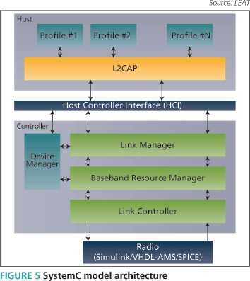
The Bluetooth specification not only defines a radio interface but also an entire communication protocol stack with the following layers (also shown graphically in Figure 5):
- Applications/Profiles. This is the upper layer of the Open System Interface (OSI) protocol stack and deals with end-user processes. Profiles defines how to use the lower Bluetooth layers to accomplish specific tasks.
- Logical Link Control and Adaptation Protocol (L2CAP). This is responsible for packet multiplexing, segmentation and reassembly.
- Host Control Interface (HCI) or Control. This defines the interface by which upper layers access lower layers of the stack.
- Link Manager Protocol (LMP). This is responsible for the link state and establishes the power control mode.
- BaseBand (BB). This deals with framing, flow control, medium access control (MAC) and mechanisms for timeout.
- Radio Frequency layer. This is concerned with the design of the Bluetooth transceiver.
Transceiver simulation from SystemC to RF
Figure 6 illustrates the modeled architecture of a Bluetooth transceiver. We focus here on one transceiver. The baseband Simulink model includes modulation/demodulation and gathers the necessary information to generate a sequence at 1Mb/s before we address the RF part of the design. The master SystemC model of the Bluetooth device master model can be substituted with a random bit generator for the RF simulation. For the RF architecture, we use a heterodyne structure with two intermediate frequencies (IF) equal to 1/3 and 2/3 of the carrier to reduce classical coupling between the voltage-controlled oscillator (VCO) and the power amplifier (PA). The frequency synthesizer is generated by a fractional phase-locked loop (PLL) [12]. The PA and the mixers are modeled both in Simulink and VHDL-AMS at different levels of abstraction.
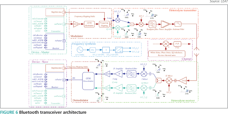
An RF transceiver contains key models (e.g., low noise amplifiers (LNAs), mixers, channel descriptions, PAs, PLLs with VCOs, filters). To simulate these elements, we need to develop a RF library [13]. This is described in a combination of VHDL-AMS behavioral language and Simulink on the ADVance System Model Extractor (ADSME) [1]. The main features of the different blocks are then characterized (e.g., the third-order intercept point and clipping effects, conversion gain, phase noise, noise figure and input/output impedances and matching).
After a first simulation, a preliminary study shows that the PA is a sensitive block. Its power consumption is by far the most important in the RF part of the design, and its power output can directly affect the transceiver (BER). For these reasons, a full SPICE description for this component is worth having. However, other blocks are described either with Simulink, VHDL-AMS or Verilog-AMS. Under the ADMS RF software, we can again mix different abstraction levels and the description languages across various parts of one block.
Simulink allows us to simulate a complete transmission system that contains RF, MAC, modems and channel by combining the digital and analog parts. We start with Simulink at the system level where it offers a baseband modeling simulation for RF systems that significantly reduces the number of simulation steps on the time domain (transient simulation).
Based on elapsed time for a 68?s Simulink simulation frame sequence, we model our transceiver by choosing from several possible simulation options (e.g., MODSST or transient) and behavioral language descriptions (e.g., SystemC, Simulink, VHDL-AMS, Verilog- AMS), and then use circuit SPICE for our PA. A final comparison with SPICE visibility can then be performed.
Several conclusions can be drawn: a Simulink design exported on ADMS runs 6x faster; one combining SystemC and Simulink on ADMS runs still 7x faster; and SystemC decreases the simulation time by 1x while behavioral languages reduce it by 2x. Armed with this information, we can determine the adequate abstraction level at which to analyze the design from SPICE to system models and estimate the bit error rate. We notice that MODSST can significantly reduce simulation time (reported as 34x [1]), but the SPICE device number must be increased to correctly use the MODSST simulation.
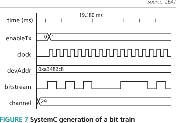
To validate our methodology, a system simulation is first done using SystemC, and the corresponding frame sequence is generated. Figure 7 shows the generation of the sequence of bits for an identification (ID) packet, the simplest packet in the Bluetooth standard.
To quickly extract estimated BER from the transceiver, an analytic model has been developed. Based on the SystemC Bluetooth frame, we simulate the transceiver including modulation, demodulation and RF architecture, with compression, frequency response and third-order harmonics characteristics extracted from previous simulations. This simulation will be done without noise in a relatively fast time. The next step will be the estimation of the BER using formula (1) [5]:
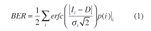
We can approximate this formula by relation to equation 2:
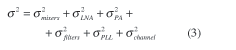
where D represents the decision level, ?i is the variance of block i, N is the number of blocks and p(i) the sequence probability, linked to the total variance (see equation 3) :
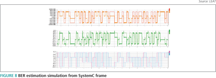
An approximation of phase noise can be done using the Allan variance [12] for mixer and PLL models or by phase noise area computation. Figure 8 presents a section from a BER analyzer simulation with the ‘cleaned’ signals (before and after modulation), variance computation and the resulting estimate for the BER.
We compute the BER using different simulations based on different hierarchical models and languages. To compare such results, we give the elapsed simulation time per bit (Xeon PC Linux, 2.8GHz and 8 Gbyte RAM) and the corresponding estimated BER:
- Ideal Simulink models (without noise): 1.4s/bit simulation time with a BER equal to 0.
- Simulink models with RF noise for the PA: 55.1s/bit simulation time with a BER equal to 6.7*10-4.
- Simulink or SystemC models for the digital part, Simulink models for the MODEM part and VHDLAMS models including noise for the RF part: 26s/bit simulation time with a BER equals to 8.1*10-4.
- Quasi-analytic BER estimation: 16ms/bit simulation time with a BER equals to 6.4*10-4.
Circuit modeling and design
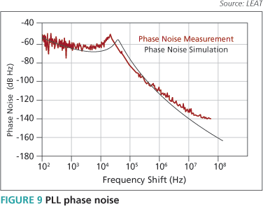
Armed with the nominal BER, one can perform RF system simulations to determine the noise performance required for each RF block (e.g., oscillator, PLL, amplifier, mixers). For example, Figure 9 shows the performance range of a PLL that can be used in Bluetooth applications—notice that the Bluetooth specification’s requirement for phase noise of -119dBc/Hz@1.5MHz is respected. A time-domain simulation, which compares different hierarchical models (using a combination of Simulink and VHDL-AMS) for the settling time, is given in Jacquemod, Geynet et al [15]. Given adequate abstraction, this simulation can be reduced by a ratio between five and six.
Conclusion
This paper demonstrated the feasibility and the efficiency of mixing analog RF and digital simulators in a single design environment. A dedicated RF design and verification platform was coupled with a SystemC emulation environment that enabled the simulation of a full Bluetooth transmit/receive flow. This started with protocol emulation followed by sent-data generation, modulation, and modeling and optimization of the RF front-end.
To achieve this, we developed a multi-language description (SystemC, Simulink, VHDL-AMS and SPICE netlist) using multiple engines (ModelSim, Matlab, Eldo and
EldoRF), across multiple domains (MAC, BB, and RF) and hierarchical description levels (system, behavioral, structural and transistor) to simulate a BT transceiver.
In comparison with other generic solutions, the simulation time is significantly decreased while the precision is increased. In addition, most of the models used for the simulations were generic, enabling easy reuse of the methodology.
References
- ADVance MS Users’ Manual, v4.5_1, AMS 2006.2
- H. De Man, F. Catthoor, G. Goossens, J. Vanhoof, J. Van Meerbergen, S. Note, J. Huisken, “Architecture-driven Synthesis Techniques for VLSI Implementation of DSP Algorithms”, Proc. IEEE, Vol. 78, no.2, 1990, pp. 319-334
- Younes Lahbib, Romain Kamdem, Mohamed-lyes Benalycherif, Rached Tourki, “An automatic ABV methodology enabling PSL assertions across SLD flow for SOCs modelled in SystemC”, Sciencedirect.com, Computers and Electrical Engineering 31 (2005), pp. 282-302, Elsevier.
- M. Zorzi, N. Speciale, G. Masetti, “A new VHDL-AMS simulation framework in Matlab”, BMAS 2002.
- P. Bontoux, I. O’Connor, F. Gaffiot, G. Jacquemod, “Behavioral modeling and simulation of optical integrated devices”, Analog Integrated Circuits and Signal Processing, vol. 29, issue 1/2, 2001, pp. 37-47
- G. Jacquemod, “Virtual RF System Platform- Myth or Reality?”, Design Automation and Test in Europe 2007, Exhibition Theatre, Technical Panel: H. Guegan, F. Lemery, Y. Deval, A. Tudose, W. Krenik, O. Vermesan, Nice, 2007
- http://www.bluetooth.com
- Matlab/Simulink User’s Manual, v2006b
- http://www.eda.org/vhdl-ams
- Modeling and Simulation for RF system design, Ronny Frevert et al., Springer 2005
- BT SIG, “Specification of the Bluetooth System – Core” Core Specification v2.1 + EDR, 2007, https://www.bluetooth.org/spec
- Clark R.L., “Phase Noise measurements on vibrating crystal filters”, Frequency Control, 1990, Proceedings of the 44th Annual Symposium, pp. 493-497
- B. Nicolle, W. Tatinian, J-J. Mayol, J. Oudinot, G. Jacquemod, “RF library based on block diagram and behavioral description”, BMAS 2007, San Jose, CA, 2007
- Clark R.L., “Phase Noise measurements on vibrating crystal filters”, Frequency Control, 1990, Proceedings of the 44th Annual Symposium, pp. 493-497
- G. Jacquemod, L. Geynet, B. Nicolle, E. de Foucauld, W. Tatinian, P. Vincent, “Design and Modelling of a Multistandard Fractional PLL in CMOS/SOI Technology”, Microelectronics Journal, 2008, vol. 39, no. 9, 2008, pp. 1130-1139
Acknowledgments
The author would like to thank the CIM-PACA Design Platform for its support.
Electronics, Antennas and Telecommunications Laboratory (LEAT)
University of Nice-Sophia Antipolis
UMR CNRS 6071
Bâtiment 4
250 rue Albert Einstein
06560 Valbonne
France
T: + 33 (0)4 92 94 28 00
W: www.elec.unice.fr
Interesting article and very informative too, actually i’m working with design and implementation of digital modulators on FPGA’s and the methodology that you exposed in the paper it’s to usefull to acquire a precise behavior of transmitters systems. An more precise aproximation is implement testbeds to characterize all the system, with all the RF domain components and observe physics nonlinearities effects over the behavioral of this components over the signal to transmit. An last question, it’s possible take some figures of your article for include in a presentation?
Kind Regards,
Alex Galaviz
Thanks for your comment. I think it is best to go back to the author for permission to reproduce the figures. A quick search on his name will find his email address readily enough.
Many thanks I’ll search the author to ask for that.