Prototyping solutions for validation of complex ASIC IP
An in-depth look at the role of FPGA-based prototyping and the validation use cases it offers when integrating complex blocks.
ASIC and SoC integration of multicore CPUs, IP blocks and increasingly sophisticated software stacks is driving demand for high-performance prototyping techniques that support extensive software development before silicon is available. Various techniques are evolving to meet this challenge. Here we focus on FPGA-based prototyping, and the features you should look for when selecting such a system.
Concurrent design
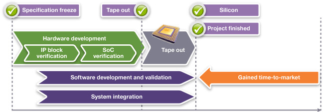
The two figures below highlight how SoC development flows are changing to enable more hardware/software design concurrency. They illustrate the context into which a modern FPGA-based prototyping system must fit.
Figure 1 shows the traditional, linear SoC development flow. Software development and system integration tasks do not begin until test silicon is available.
Figure 1 Traditional serial SoC development project (Source: Synopsys)
Figure 2 shows the newer flow being adopted to enable more parallel development. It allows design teams to validate IP blocks or entire SoC systems using the software elements of the design before silicon arrives. The result is a critical gain in time-to-market.
Figure 2 Parallel SoC development project (source: Synopsys)
FPGAs provide an excellent platform for the newer flow of their capacity, programmability, and flexible I/O interfaces. Integrated into the right kind of prototyping system, they address the fundamental challenges presented by concurrent design.
The challenges of complex IP prototyping
One example of prototyping system integration is the use of 28nm Virtex-7 690T devices from Xilinx at the heart of the HAPS Developer eXpress system (HAPS-DX), part of the Synopsys HAPS family of FPGA prototyping boards. With approximately 4 million ASIC gates of capacity and a variety of I/O resources, the 690T is well suited to a range of IP validation scenarios. The HAPS system integrates these devices in a ruggedized electro-mechanical enclosure, with heat management, a flexible connector-cable-socket scheme, and design automation software tailored for automating prototyping tasks.
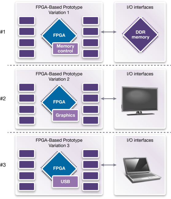
One challenge of FPGA-based prototyping is to create a cost-effective implementation that supports many verification strategies. Figure 3 shows three strategies a prototype may need to support during development.
Figure 3 Prototype variations for IP validation (Source: Synopsys)
Each of these strategies is likely to call for a variety of PHYs, FPGA I/O configurations, and interface accessory hardware.
There are then two common IP validation scenarios that a prototype must support: re-validation and integration.
In a re-validation scenario, the prototype should provide a platform on which the design team can explore the functionality of a particular IP implementation. For example, the Synopsys DesignWare IP for a USB 3.0 interface is offered as both the controller and the PHY and then may be applied as an extensible host controller interface (xHCI), a mass-storage device, or in On-The-Go (OTG) format for hosting. A design team will use a system like HAPS-DX to confirm the functions of the controller configuration, controller-to-PHY operation, PHY electrical compliance and driver development.
In an integration scenario, the FPGA-based prototype must serve as a platform for the integration of multiple IP blocks or as a way of combining a new block with a processor subsystem. Software can be applied to confirm peripheral access, measure access latency, and confirm that software algorithms operate as expected across real-world interfaces connected to the prototype.
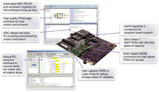
To provide a balance of high-performance interface flexibility and sufficient capacity for ASIC IP, the prototyping platform must support many interface specifications and provide design automation to make IP migration as easy as possible. HAPS-DX incorporates a capable FPGA, flexible I/O architecture, and software that automates the bring-up and debug tasks. Figure 4 is an overview of the system’s hardware and software elements.
Figure 4 HAPS-DX system overview (Source: Synopsys)
Other major features of the HAPS-DX include:
- I/O interfaces compatible with both industry-standard FPGA Mezzanine Card (FMC) and HAPS HapsTrak 3 formats
- Linux-compatible prototype automation and debug software
- HDL compilers that support popular formats, recognize synthesis coding styles, and DesignWare IP
- Support for Synopsys Design Constraints (SDC) and Universal Power Format (UPF)
- Fast HDL compiler modes which reduce the review time of RTL and provide up to four times greater throughput than traditional FPGA synthesis tools
- RTL debug and high-capacity storage options provide up to 4Gbyte of storage
- Integrated Universal Multi-Resource Bus (UMRBus) hardware interface and C/C++/Tcl APIs
I/O interfaces and daughter board selection
An FPGA-based prototyping system must have an I/O architecture that supports many real-world interfaces, so that users can validate the functionality and review the quality of a design-under-test (DUT) in the context of these interfaces. To bring up prototypes quickly, design teams need to have access to pre-engineered interfaces rather than building their own.
The HAPS-DX system has HapsTrak sockets and a HapsTrak to FPGA Mezzanine Card (FMC) adapter. Synopsys HAPS daughter boards support standard I/O protocols like USB, DVI, and PCI Express as well as memories such as SRAM and DDR. FMC standard cards are available for AD/DA conversion, serial connectivity, image processing, radio interfaces and motor control.
The FPGA Mezzanine Card (FMC) is an ANSI-standard mezzanine card form factor, connectors, and modular interface to an FPGA located on a carrier board such as the HAPS-DX. Decoupling the I/O interfaces from the FPGA simplifies interface module design and maximizes carrier card reuse. The HAPS-DX system supports two HapsTrak 3 to FMC adapters, each of which provides an interface to an FMC High Pin Count connector with 400 pins as well as access to the 160 single-ended I/Os and 10 differential GTH I/Os available on the Virtex-7 690T.
Prototype use modes
State-of-the-art FPGA-based prototypes can be operated stand-alone or connected to a workstation to take advantage of PC-based computing resources as part of the implementation. The HAPS-DX system can be used in three main ways: standalone, PCIe connected, or as a component in a hybrid prototype.
Standalone prototyping
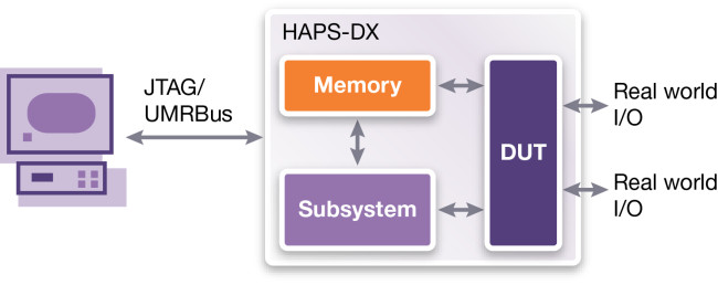
IP block validation is the most popular application for FPGA-based prototypes because their real-time clock performance and connectivity to high-fidelity interfaces make them ideal self-contained validation environments for many DUTs. In this use mode it is common for an embedded CPU subsystem of the prototype design to act as a test jig executing the software stack. In a HAPS-DX environment, FMC or HapsTrak 3 daughter boards provide PHY interfaces for a wide variety of protocols and systems and the HAPS-DX itself provides connectivity via JTAG to external workstations running the software Integrated Development Environment (IDE).
Figure 5 Standalone prototype use mode (Source: Synopsys)
PCI Express connected prototyping
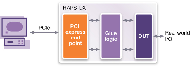
A prototype system plugged into the PCIe slot of a host workstation can take advantage of high-volume data streaming to a DUT (This is a popular way of validating the quality of media controllers.) In the HAPS-DX system, the PCIe paddle board and end-point core eases memory-mapped access to the DUT. The HAPS UMRBus provides the API, so custom applications can communicate with, and control, logic on the DUT. DUT connections are made within the RTL using a simple client interface module.
Figure 6 PCIe connected prototype use mode (Source: Synopsys)
Hybrid prototyping
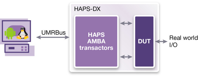
A prototyping system that can mix SystemC/transaction-level models with FPGA-based prototype hardware provides a way to make prototypes available earlier in the design cycle, even before RTL is available. A virtual prototype communicates to the RTL DUT via bus protocol transactors to bridge loosely-timed models with cycle-accurate hardware. The DUT RTL is validated in the context of a virtual-processor subsystem running a software stack comprised of OS and application software.
Figure 7 Hybrid prototype use mode (Source: Synopsys)
Note that a single ASIC/SoC prototyping project may use a number of these approaches at once.
Design visibility of the prototype
Because prototypes can run at multiple megahertz, they can reach system states that would not be feasible using a traditional verification tool such as an HDL simulator. If an RTL bug is exposed during IP block validation, prototype teams need a robust way to help troubleshoot internal operation.
IP block validation involves observation of block functions or quality review of processed data outside the prototype. The ability to instrument and probe internal signal states and intermediate data streams can help a team understand unexpected results and troubleshoot bugs that may have slipped through the RTL/IP verification phase.
HAPS-DX was designed to have a non-intrusive approach to debug so that it is not necessary to change the ‘golden’ ASIC RTL code to add visibility to the prototype. Once the target FPGA is programmed, an RTL debugger application running on a workstation communicates with the FPGA via the HAPS UMRBus or JTAG interface to set trigger modes and view captured data of the live system.
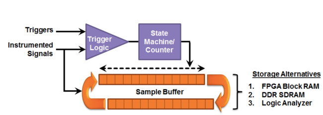
The basic trigger and buffer system of the HAPS-DX RTL debugger is shown in Figure 8. Triggers and instrumented signals originate from the DUT and feed the trigger condition logic that enables the recording of state events in a flexible sample buffer. The frequency of event recording can be controlled with state machine or counter logic to isolate periods of interest.
Figure 8 HAPS-DX debug logic architecture (Source: Synopsys)
Different debug scenarios will require different types of sample buffer memory, depending on how long a period must be captured to review a function, or the number of signals that must be monitored. Debug storage may be assigned to FPGA Block RAM, DDR3 memory installed on the HAPS-DX system board, or an external logic analyzer.
Summary
Design teams evaluating FPGA-based prototyping systems for IP block validation should consider the variety of physical interfaces that are available and the flexibility with which they can be used. They should also look for a robust hardware architecture and integrated automation tools so that the systems can start delivering results quickly in a wide variety of verification scenarios.
About the author
Troy Scott, product marketing manager, is responsible for FPGA-based prototyping software tools at Synopsys. He has 20 years of experience in the EDA and semiconductor industry. His background includes HDL synthesis and simulation, SoC prototyping, and IP evaluation and marketing.

